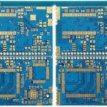
When selecting a PCB manufacturing company, technical expertise, production capability, quality control, and supply chain reliability are all important factors to consider. A qualified PCB manufacturer should not only be able to fabricate standard circuit boards but also provide the engineering support and manufacturing flexibility required for complex electronic products.
Kingda provides professional PCB manufacturing, PCB prototyping, and PCB assembly solutions for customers developing and producing electronic products. By combining rapid prototyping capabilities with reliable PCB fabrication and assembly services, Kingda helps customers move from initial design validation to production more efficiently.
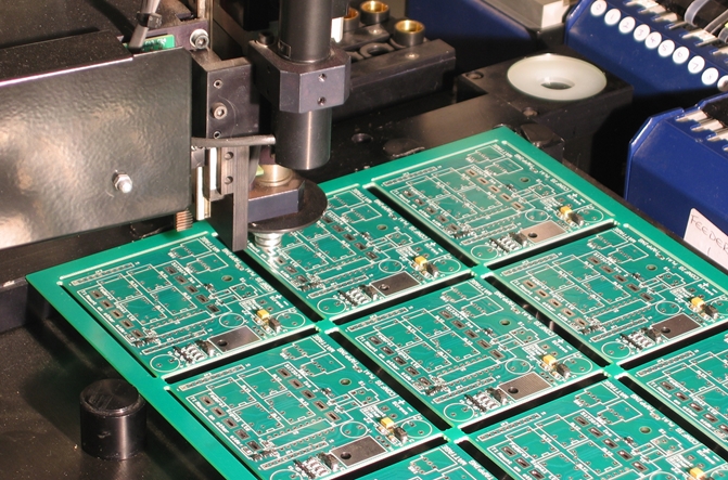
For projects involving complex multilayer structures, HDI circuit boards, fine-pitch components, advanced surface finishes, or customized production requirements, choosing an experienced manufacturing partner can reduce development risks and improve overall project efficiency.
Kingda PCB Manufacturer for Prototype and Production
A successful PCB project often begins long before the manufacturing process. Design verification, material selection, stack-up planning, manufacturability analysis, and component sourcing can all influence the final cost, quality, and production schedule.
Kingda supports customers throughout these stages with integrated PCB manufacturing and PCB assembly capabilities. Instead of treating PCB fabrication and assembly as completely separate processes, an integrated manufacturing approach allows engineers and customers to coordinate design requirements, fabrication specifications, component requirements, and assembly processes more effectively.
Kingda’s services can support different stages of the product lifecycle, including:
- PCB prototype manufacturing
- Rapid PCB prototyping
- Multilayer PCB manufacturing
- HDI PCB manufacturing
- Rigid PCB fabrication
- Flexible and rigid-flex PCB solutions
- PCB assembly
- SMT assembly
- Through-hole assembly
- Component sourcing
- DFM and engineering support
- Functional and electrical testing
This flexible model allows customers to work with one manufacturing partner from prototype development through production rather than coordinating multiple suppliers for different stages.
HDI Circuit Board Manufacturing Expertise
As electronic products become smaller and more powerful, designers increasingly need higher routing density within limited board dimensions. HDI circuit boards provide an effective solution by incorporating technologies such as microvias, blind vias, buried vias, and sequential lamination.
Kingda supports advanced HDI PCB manufacturing for applications where compact dimensions, high interconnect density, and reliable electrical performance are important.
Compared with conventional through-hole structures, microvia technology can provide greater routing flexibility and allow designers to make better use of limited PCB space. Depending on the design, HDI structures can help optimize component placement, signal routing, and overall board size.
Key HDI manufacturing technologies may include:
- Laser-drilled microvias
- Blind and buried vias
- Sequential lamination
- Fine-line circuitry
- High-density multilayer structures
- Controlled impedance routing
- Advanced PCB stack-up design
For high-speed and high-density electronic products, PCB manufacturing must consider more than simply achieving the required dimensions. Signal integrity, dielectric material selection, copper distribution, impedance control, thermal management, and via reliability must also be addressed during the design and manufacturing stages.
Kingda’s engineering-oriented approach helps customers evaluate these factors before production, reducing the risk of manufacturing problems during later stages.
ENIG and Immersion Silver PCB Surface Finishes
Surface finish is another important consideration when selecting a PCB manufacturer. The appropriate finish can affect solderability, surface protection, component compatibility, reliability, and overall manufacturing cost.
Kingda supports advanced surface-finish options such as ENIG (Electroless Nickel Immersion Gold) and Immersion Silver, depending on project requirements.
ENIG PCB
ENIG PCB technology provides a relatively flat surface that is well suited to fine-pitch components, BGA packages, and high-density circuit boards.
The immersion gold layer protects the nickel surface from oxidation and provides good solderability. Its flatness also makes ENIG a popular option for applications where precise component placement and reliable solder joints are required.
Immersion Silver PCB
Immersion Silver PCB provides a thin, conductive surface finish with good solderability. It can be considered for applications where electrical performance, surface flatness, and cost need to be balanced.
The selection between ENIG, immersion silver, OSP, HASL, and other finishes should be based on the PCB design, assembly process, environmental conditions, component requirements, and expected product lifetime.
Kingda can help customers evaluate surface-finish requirements during the engineering and quotation stages to select an appropriate manufacturing solution.
Rapid PCB Prototyping for Faster Product Development
PCB prototypes are essential for validating electronic designs before moving into larger production quantities. A prototype allows engineers to verify electrical functionality, component placement, mechanical dimensions, signal performance, thermal behavior, and manufacturability.
Kingda provides rapid PCB prototyping services designed to help customers shorten development cycles and identify potential problems earlier.
An efficient prototyping process can provide several benefits:
Faster design validation:
Customers can obtain prototype boards and evaluate the design before committing to larger production volumes.
Reduced development risk:
Early manufacturing feedback can reveal problems related to trace spacing, drill sizes, copper distribution, stack-up configuration, or component placement.
Improved DFM performance:
Design-for-manufacturing analysis helps ensure that the PCB design is compatible with the selected manufacturing process.
Smoother transition to production:
Using the same manufacturing partner for prototypes and production can simplify communication and reduce the possibility of process inconsistencies.
For startups, engineering teams, and established electronics manufacturers, rapid prototyping can be particularly valuable when products require multiple design iterations.
Kingda PCB Assembly and End-to-End Manufacturing
PCB fabrication is only one part of the electronics manufacturing process. Once the bare PCB is produced, components must be accurately placed, soldered, inspected, and tested to create a functional PCBA.
Kingda extends its manufacturing capabilities beyond PCB fabrication by providing PCB assembly services.
Depending on project requirements, PCB assembly may include:
- Component procurement
- BOM verification
- SMT assembly
- Through-hole assembly
- Solder paste printing
- Component placement
- Reflow soldering
- Wave soldering
- AOI inspection
- X-ray inspection
- Electrical testing
- Functional testing
- Final assembly
By combining PCB manufacturing and PCB assembly, Kingda can provide customers with a more streamlined supply chain.
This integrated approach can reduce the number of external suppliers involved in a project, simplify communication, and make it easier to coordinate PCB specifications with component and assembly requirements.
PCB Manufacturing Quality Control
Quality is a critical factor in PCB manufacturing, particularly for products used in demanding industrial, medical, automotive, telecommunications, and other applications.
Kingda emphasizes process control throughout PCB fabrication and assembly. Depending on the project, quality assurance can include incoming material inspection, process monitoring, automated inspection, electrical testing, and final quality verification.
Typical PCB quality-control processes include:
- Design and DFM review
- Incoming material inspection
- Automated optical inspection (AOI)
- Solder paste inspection (SPI)
- X-ray inspection
- Electrical testing
- Dimensional inspection
- Impedance testing
- Visual inspection
- Final quality inspection
For customers requiring consistent production, traceability and process documentation are also important. A structured quality system can help identify manufacturing deviations and provide greater visibility throughout the production process.
Cost Optimization in PCB Manufacturing
The lowest initial quotation does not always represent the lowest total PCB manufacturing cost.
PCB pricing can be influenced by numerous factors, including:
- PCB material
- Number of layers
- Board dimensions
- Copper thickness
- Minimum trace and spacing
- Via structure
- Surface finish
- Order quantity
- Panel utilization
- Component availability
- Assembly complexity
- Testing requirements
Kingda works with customers to evaluate these factors during the engineering and quotation stages.
For example, optimizing panel utilization can reduce material waste, while selecting an appropriate stack-up and via structure can help balance PCB performance with manufacturing complexity.
For HDI PCB manufacturing, cost optimization is especially important because microvias, sequential lamination, fine-line structures, and specialized materials can increase manufacturing complexity.
A professional PCB manufacturer should therefore focus not simply on reducing the unit price but on optimizing the complete manufacturing process while maintaining the required quality and performance.
PCB Manufacturing for Multiple Industries
Modern PCB technology is used across virtually every major electronics sector. Kingda’s manufacturing and assembly capabilities can support projects with different technical and production requirements.
Medical Electronics
Medical electronics require reliable circuit boards with consistent manufacturing quality. PCB manufacturing for medical applications may involve strict material, cleanliness, traceability, and inspection requirements.
Automotive Electronics
Automotive systems increasingly rely on sophisticated electronic control units, battery-management systems, sensors, ADAS equipment, and infotainment systems. These applications can require high-reliability multilayer and HDI PCB technologies.
Telecommunications
High-speed communication equipment requires careful control of signal integrity and impedance. Advanced multilayer and HDI PCB technologies can help designers achieve higher routing density while maintaining electrical performance.
Industrial Electronics
Industrial control systems, automation equipment, instrumentation, and power electronics often require durable PCBs capable of stable operation under demanding conditions.
Consumer Electronics
Compact consumer products frequently require smaller PCB dimensions, high component density, and cost-effective production. HDI and multilayer technologies can help manufacturers meet these requirements.
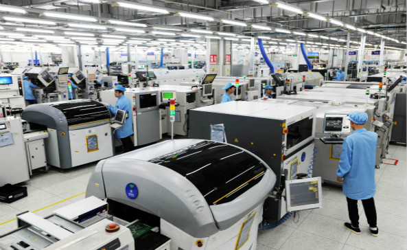
From PCB Prototype to Volume Production
One of Kingda’s key advantages is the ability to support customers across different stages of product development.
The manufacturing process can be viewed as a complete workflow:
PCB Design → DFM Review → PCB Prototype → Design Validation → PCB Fabrication → Component Sourcing → PCB Assembly → Testing → Production
This approach helps customers maintain continuity as their products progress from engineering samples to commercial production.
For new product development, the prototype stage can be used to identify design and manufacturing issues. Once the design has been validated, production processes can then be optimized for repeatability, quality, and cost efficiency.
Having access to both PCB prototype manufacturing and PCB assembly also reduces the need to transfer designs between different suppliers during the development cycle.
Why Choose Kingda as Your PCB Manufacturing Partner?
Selecting a PCB supplier requires more than comparing quotations. Customers should consider technical capabilities, manufacturing flexibility, engineering support, quality control, production scalability, and communication.
Kingda provides several advantages for customers looking for an integrated electronics manufacturing partner:
1. Rapid PCB Prototyping
Kingda’s rapid PCB prototyping capability helps engineering teams validate designs quickly and move efficiently toward production.
2. Professional PCB Manufacturing
Kingda supports a range of PCB technologies, including multilayer boards and advanced HDI circuit boards, helping customers manufacture increasingly complex electronic designs.
3. PCB Assembly Integration
Combining PCB fabrication with PCB assembly allows customers to simplify procurement and production management through an integrated manufacturing workflow.
4. Engineering and DFM Support
Early engineering review can identify potential manufacturing problems before fabrication, helping reduce unnecessary redesigns and production delays.
5. Flexible Production
Kingda can support projects ranging from prototype quantities and small batches to larger production requirements, allowing customers to scale their manufacturing as product demand develops.
6. Quality-Focused Manufacturing
Inspection and testing throughout the manufacturing process help ensure that finished PCBs and PCB assemblies meet the required technical specifications.
7. One-Stop Electronics Manufacturing
By integrating PCB fabrication, component sourcing, assembly, and testing, Kingda provides a convenient end-to-end PCB manufacturing solution for customers seeking to simplify their supply chain.
Conclusion
Choosing the right PCB manufacturing company is an important part of developing reliable electronic products. A capable supplier should provide more than bare-board fabrication. It should also offer engineering support, rapid prototyping, quality control, scalable production, and assembly capabilities.
Kingda combines PCB manufacturing, HDI PCB manufacturing, rapid PCB prototyping, and PCB assembly to support customers throughout the product development lifecycle. From initial design review and prototype fabrication to component sourcing, assembly, testing, and production, an integrated manufacturing model can help reduce supply-chain complexity and improve project efficiency.
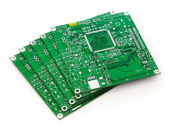
For companies developing high-density, compact, and performance-driven electronic products, technologies such as HDI circuit boards, ENIG PCB, and Immersion Silver PCB provide valuable options for meeting demanding design requirements.
Ultimately, the right PCB manufacturing partner should be evaluated not only by price, but also by engineering expertise, manufacturing quality, responsiveness, scalability, and the ability to support the complete journey from prototype to production. With its integrated manufacturing approach and focus on flexible PCB solutions, Kingda can serve as a reliable partner for businesses seeking efficient and professional PCB manufacturing and assembly services.