Lead-Free Soldering in PCBA: Complete GuideLead
As environmental regulations continue to influence electronics manufacturing, soldering technology has undergone a major transformation. Lead-Free Soldering has become the standard choice for many electronic products, while leaded solder remains relevant in specific applications where its processing characteristics and reliability advantages are important.
Choosing between lead-free and leaded soldering is not simply a matter of selecting a solder alloy. Engineers must also consider thermal profiles, component compatibility, PCB materials, solder joint reliability, regulatory requirements, and production costs.
Understanding these differences helps manufacturers select the right PCBA Soldering process for a specific electronic product.
Lead-Free vs Leaded Soldering: Key Differences
The most important differences between lead-free and leaded soldering involve solder composition, melting temperature, processing requirements, mechanical properties, and regulatory compliance.
Lead-Free Soldering
Lead-free solder typically uses alloys based on tin combined with elements such as silver and copper. Common SAC alloys are widely used in modern electronics manufacturing.
Compared with traditional Sn-Pb solder, lead-free alloys generally have a higher melting temperature. Many commonly used lead-free alloys melt at approximately 217–227°C.
This higher melting temperature requires more carefully controlled reflow profiles and places greater thermal demands on components and PCB assemblies.
Leaded Soldering
Traditional leaded solder commonly uses tin-lead alloys. Sn63/Pb37, for example, has a melting point of approximately 183°C.
The lower processing temperature makes leaded solder easier to process and can reduce thermal stress on certain components.
Leaded solder also has favorable wetting characteristics and has historically been widely used for reliable solder joint formation.
However, the use of lead is restricted in many commercial electronics applications because of environmental and regulatory requirements.
Three Major Challenges of Lead-Free Soldering
Although lead-free soldering provides important environmental benefits, it introduces several manufacturing challenges that must be carefully controlled.
1. Narrower Thermal Process Window
The higher melting temperature of lead-free solder requires a higher reflow temperature.
A suitable thermal profile must provide sufficient heat for complete solder melting while avoiding excessive thermal stress on components and PCB materials.
An improperly optimized profile can result in defects such as:
- Insufficient soldering
- Poor wetting
- Component damage
- Solder bridging
- Tombstoning
- Excessive thermal stress
For this reason, thermal profiling is an important part of reliable PCB Assembly.
2. Solder Joint Reliability
Lead-free solder alloys can have different mechanical and fatigue characteristics compared with traditional Sn-Pb solder.
Under repeated thermal cycling, vibration, or mechanical stress, solder joints may experience fatigue over time.
The actual reliability depends on many factors, including solder alloy, component package, PCB design, pad geometry, thermal cycling conditions, and assembly process control.
Proper process design and inspection are therefore essential for applications where long-term reliability is critical.
3. Component and Material Compatibility
Not every component is equally tolerant of the higher temperatures associated with lead-free soldering.
Engineers should verify:
- Component temperature ratings
- PCB material specifications
- Surface finish compatibility
- Solder mask performance
- Moisture sensitivity
- Thermal profile limitations
Early engineering review can identify potential compatibility problems before production.
A well-designed PCB Design & Layout process can help optimize pad structures, component spacing, thermal management, and manufacturability before assembly begins.
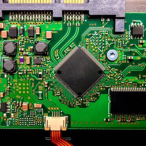
Lead-Free vs Leaded Soldering Comparison
| Characteristic | Lead-Free Soldering | Leaded Soldering |
|---|---|---|
| Typical alloy | SAC and other Pb-free alloys | Sn-Pb alloys |
| Melting temperature | Generally higher | Generally lower |
| Thermal demand | Higher | Lower |
| Wetting characteristics | Good but process-sensitive | Excellent |
| Environmental compliance | Better suited to restricted-substance requirements | Restricted in many applications |
| Process control | More demanding | Generally easier |
| Thermal stress | Potentially higher | Generally lower |
| Common applications | Consumer, industrial, automotive, medical and other regulated products | Certain legacy, specialized, and exempt applications |
The choice should always be based on the product’s regulatory requirements, reliability targets, component specifications, and manufacturing conditions.
How Manufacturers Control Lead-Free Soldering Quality
A reliable lead-free process requires more than simply changing the solder material. Each stage of production must be controlled.
Optimize the Reflow Profile
The reflow profile should be developed according to the solder paste manufacturer’s specifications and the thermal limitations of the PCB assembly.
Important parameters include:
- Preheating rate
- Soak temperature
- Time above liquidus
- Peak temperature
- Cooling rate
An optimized profile helps achieve consistent solder joints while minimizing thermal damage.
Use Automated Inspection
Automated inspection technologies can identify many soldering and placement defects.
Depending on the product, inspection may include:
- Solder Paste Inspection (SPI)
- Automated Optical Inspection (AOI)
- X-ray inspection
- Visual inspection
- Electrical testing
X-ray inspection is particularly useful for hidden solder joints such as BGAs and other bottom-terminated components.
Control Through-Hole Soldering
Lead-free requirements also affect through-hole assembly.
Wave soldering and selective soldering processes must be adjusted for the characteristics of lead-free solder alloys.
For assemblies containing both surface-mount and through-hole components, Mixed Technology PCB Assembly can coordinate multiple assembly technologies within the same manufacturing workflow.
Lead-Free Soldering and PCB Design
Soldering reliability starts before the PCB enters the production line.
PCB designers should consider soldering requirements during the design stage, including:
- Pad dimensions
- Component spacing
- Thermal relief
- Copper distribution
- Component orientation
- Solder mask design
- Thermal management
- Accessibility for inspection and testing
Uneven copper distribution, for example, can create thermal imbalances during reflow and affect solder joint formation.
Design-for-manufacturing principles can help identify these problems before production.
When Is Leaded Solder Still Used?
Although lead-free solder is widely adopted, leaded solder has not disappeared completely.
It may still be used in applications where regulations permit it or where specific technical requirements justify its use.
Potential considerations include:
- Legacy product designs
- Specialized electronics
- Certain high-reliability applications
- Specific repair and rework requirements
- Applications covered by regulatory exemptions
However, manufacturers should always verify the applicable environmental regulations and customer requirements before selecting a leaded solder process.
Choosing the Right Soldering Process for PCBA
The best soldering process depends on the complete product requirement rather than solder composition alone.
For Regulated Commercial Electronics
Lead-free soldering is generally the preferred approach because it supports compliance with environmental requirements applicable to many markets and product categories.
For High-Reliability Electronics
Engineers should evaluate solder alloy performance together with component selection, PCB design, thermal cycling, vibration, mechanical stress, and the required product lifetime.
The solder alloy is only one part of the overall reliability equation.
For Mixed SMT and THT Assemblies
Products containing both surface-mount and through-hole components may require multiple soldering processes.
A combination of reflow soldering, wave soldering, selective soldering, and manual rework may be used depending on the PCB design.
GOPCBA’s Through-Hole PCB Assembly capabilities can support projects where through-hole components must be integrated with the broader PCBA process.
Why Process Control Matters More Than Solder Type Alone
Whether a product uses lead-free or leaded solder, manufacturing quality depends heavily on process control.
A reliable PCBA manufacturing process should address:
- Material selection
- PCB design and manufacturability
- Solder paste control
- Component placement
- Thermal profiling
- Soldering parameters
- Automated inspection
- Electrical and functional testing
- Rework management
- Final quality verification
For prototype and low-volume projects, process optimization is especially important because design changes can often be identified and corrected before larger production runs.
GOPCBA can support the transition from prototype validation to production through Rapid PCBA Prototyping and related PCB assembly services.
Conclusion
Lead-free and leaded soldering each have distinct technical characteristics.
Lead-Free Soldering offers important environmental and regulatory advantages but generally requires higher processing temperatures and tighter thermal process control. Leaded Soldering provides excellent wetting, a lower melting temperature, and established processing characteristics, but its use is restricted in many applications.
For modern electronics manufacturing, lead-free solder is generally the preferred option when regulatory requirements apply. However, the final decision should consider the complete product design, component limitations, reliability requirements, applicable regulations, and manufacturing process.
The most reliable results come from treating soldering as part of an integrated PCBA manufacturing process—from PCB design and material selection through assembly, inspection, and testing.