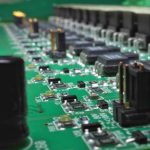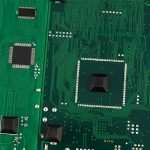
Miniaturized Medical PCB Manufacturing for Implants
Implantable devices keep shrinking while their electronic workload grows. Cardiac monitors, neurostimulators and sensing platforms must fit sensing, processing, communication and power management into very small spaces. The circuit board sits at the center of that squeeze. A miniaturized medical PCB carries far less routing room than a conventional board. Yet it must still hold its electrical performance, mechanical integrity and reliability. Small process drift that a normal board would absorb can become a large yield loss here.
This guide covers the design choices, fabrication risks and verification steps that decide whether a compact implantable board can be built in volume. Each section explains what the decision changes on the floor. It also lists what a buyer or engineer should check before release. The focus stays on process causes and tradeoffs, not on headline capability numbers.
Why Miniaturization Matters
The size and weight of the electronics shape the whole mechanical design of an implantable device. Trimming board area can give engineers room for the enclosure, the battery and the feedthroughs. It also shortens signal paths and can reduce the number of connectors inside the package. None of this comes free. The same circuit functions must still work while routing space falls. Designers therefore trade layer count, feature size and component pitch against each other.
The goal is higher functional density with a reliability margin that still holds after years in the body. That balance should be set early, before the first article is built. A margin chosen on paper may not survive real production panels. Engineers should agree the limits with the fabricator and record them in the drawing. Those limits then guide every later check, from imaging to final test.
Space and Routing Pressure
A conventional board usually has spare area for components, connectors and test structures. Implantable electronics rarely enjoy that luxury. Traditional routing habits become inefficient when the available outline is tight. An advanced miniaturized medical PCB may need fine-line routing, smaller vias, sequential build-up and dense component placement to fit the circuit. Each of those choices narrows the process window. The manufacturer must then hold tight control over dimensional accuracy and registration between layers.
Buyers should confirm that the supplier can hold those limits on real production panels, not only on a sample. Ask for the process sheet that lists the agreed values. Ask how the line reacts when a parameter drifts outside its window. A supplier that answers with data is easier to compare than one that answers with a brochure. A capable PCB design and layout review helps match the stackup to the supplier’s proven process.
Fine-Line Fabrication Limits
As board dimensions fall, circuit density rises, and fine-line structures allow more connections in less area. Smaller features also shrink every manufacturing margin. Small variations in imaging, etching, lamination, drilling or registration have a larger effect on the finished circuit. A trace that etches slightly wide may reduce spacing below the design value. A pad that shifts during lamination may miss its via target. These are ordinary process effects, not rare accidents.
Miniaturized production therefore needs a process that keeps line geometry, pad dimensions, via structures and layer alignment consistent across the lot. Ask how the supplier monitors these parameters and what data it keeps for each build. The answer should name the measurement, the frequency and the person who reviews it. Without that loop, a drift is found only when boards fail test.
HDI Technology and Microvias
High-density interconnect is one of the most useful technologies for compact electronics. An HDI medical PCB uses microvias, blind and buried vias, fine lines and small pads to create more efficient interconnections. Compared with conventional multilayer construction, HDI can raise wiring density, shorten electrical paths and use board space more efficiently. It also supports fine-pitch components and compact packaging. For implantable work, the right HDI structure should follow the device requirements rather than a headline capability number.
Electrical, mechanical, manufacturing and reliability needs all shape the stackup. A simple build-up with fewer sequential steps is easier to control than a deep one. Each added lamination cycle brings another registration risk and another chance for trapped material. Engineers should choose the least complex structure that meets the routing need. That choice usually lowers cost and improves yield at the same time.
Microvia Reliability Factors
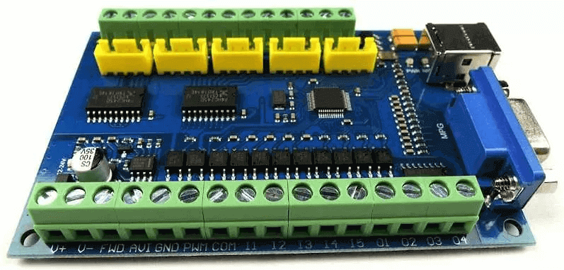
Microvias connect specific layers within a build-up structure instead of passing through the whole board. That frees routing space and reduces via footprint, which helps with fine-pitch parts. Reliability depends on material selection, aspect ratio, laser-drilling quality, copper plating and filling. Thermal and mechanical design matter too. A theoretical minimum via size means little if the plating or fill is inconsistent. Microvia design should be evaluated against the manufacturer’s actual production capability.
Engineers should request cross-section data and inspection records before approving a via structure for an implantable build. The cross-section shows plating thickness, fill quality and target alignment in one view. Inspection records show whether those results repeat across the lot. Both belong in the first-article package. A supplier with quality management discipline will tie these checks to its process records.
Material Selection for Implants
Material choice becomes more important as features shrink. Designers may consider medical-grade FR-4, polyimide-based flexible materials, high-TG laminates and specialized substrates. The right material follows the electrical, mechanical, thermal and packaging requirements of the device. Engineers should weigh dielectric performance, dimensional stability, thermal expansion, moisture resistance and copper adhesion. Layer thickness and flexibility also affect how the board behaves during assembly and in service. For some implantable applications, the board is integrated into a hermetic or otherwise protected package.
Biocompatibility, sterilization and body-contact safety must be evaluated at the finished-device level, not assumed from the laminate alone. The PCB material is one part of a material system. The package, the coating and the assembly process all interact with it. Buyers should keep those questions with the device risk file. The fabricator can supply material data, but it cannot certify the finished implant.
Flexible and Rigid-Flex Options
Not every implantable device is best served by a rigid board. When circuits must follow a curved or constrained structure, flexible and rigid-flex technology can add design freedom. A rigid-flex medical PCB combines rigid sections with flexible circuits in one integrated structure. This can cut connectors, cables, wiring interfaces and assembly space. Fewer interconnection points also mean fewer places for a joint to fail. The flexible portion must still be designed around bend radius, copper construction, layer count and mechanical stress.
The intended packaging environment decides how much bending the flex region can safely take. A flex area that is folded once during assembly faces different stress than one that moves in service. Buyers should confirm that the supplier builds both rigid and flex sections under one process flow. Splitting the work between two factories adds handling steps and hides responsibility when a defect appears.
Signal Integrity in Dense Boards
Miniaturization should never cost signal quality. Implantable electronics may handle low-level sensor signals, stimulation pulses, digital data and wireless links. As traces sit closer together, unwanted coupling and noise become easier to create. Sensitive analog paths should stay away from major noise sources where practical. Short signal paths, clean grounding, power filtering and controlled return currents all help. Separating analog and digital sections reduces interference. Where high-speed interfaces exist, controlled impedance and differential-pair routing may be required.
Stackup, dielectric thickness, copper geometry and reference planes should be considered together. A change to one of them shifts the others. The fabricator should confirm the impedance target against its own stackup before release. Test coupons on the production panel can then verify the result. That step turns an electrical assumption into a measured number the buyer can review.
Process Control and Inspection
The smaller the feature, the more manufacturing variation matters. Imaging must transfer design data onto copper accurately, because etching then defines the final conductor geometry. Over-etching or under-etching changes trace width and spacing. For HDI structures, laser drilling creates the microvias, and drilling accuracy, hole shape and plating all affect interconnection reliability. Multilayer and HDI boards also need accurate registration between layers. Even small errors can shift pads, vias and traces away from their targets.
Controlled lamination parameters protect dimensional stability and interlayer alignment. Production control should cover the whole chain, from incoming material to final test, with records kept for each lot. Buyers should ask which parameters are recorded and who reviews the trend. A recorded number that nobody reads does not control anything. The review habit is what turns data into a stable process.
Quality and Traceability
Reliability demands are high because an implanted device may be hard or impossible to access later. Manufacturing consistency therefore carries real weight. A sound quality program may include incoming material inspection, material traceability, DFM review, dimensional checks, AOI, X-ray, electrical continuity and insulation testing. Microvia inspection and cross-section analysis add confidence in the build-up layers. Assembly inspection and functional testing close the loop. The exact inspection plan should follow the finished device, customer specifications and the risk-management process.
Buyers should ask which tests run on every lot and which run only on the first article. That split decides how much protection a repeat order really gets. Manufacturing records then show how a specific board was produced. Depending on the project, traceability may cover raw material batches, PCB production records, component lot information and assembly parameters. Inspection results, electrical test data and revisions belong in the same file. A supplier that can pull the full record for a serial number is easier to work with during an audit.
Assembly Fit and Volume Planning
Fabrication and assembly must be planned together. As boards shrink, component packages get smaller and spacing gets tighter. Solder-paste printing, placement accuracy, reflow control and inspection all become more critical. Medical assembly may involve fine-pitch SMT, micro-BGA, CSP and mixed SMT and through-hole work. Automated optical inspection and X-ray catch joints that visual checks miss. Reliable turnkey PCB assembly keeps fabrication and assembly under one process owner. That matters because a stencil or profile change on one side affects yield on the other.
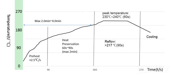
Coordinated development beats two independent steps. The reflow profile is a good example. A profile that suits a large board may overheat a thin implantable one. The paste, the stencil and the oven curve should be tuned to the actual board. Buyers should ask when that tuning happens and who signs it off. For volume programs, high-volume PCB assembly planning should start while the prototype is still under review.
Component supply deserves the same attention. A part that quietly changes plating, a paste batch with different viscosity or a reel stored in humidity can shift the process without any machine warning. Qualified materials, certificates of analysis and approved alternates keep a supply change from becoming a quality incident. Sound component procurement includes lot tracking and incoming checks that feed the traceability file. Small packages leave little room for a substitute part that behaves differently.
Miniaturized medical electronics usually need serious engineering verification before production. A practical workflow starts with a design review of the board, stackup, materials, components and mechanical dimensions. DFM and DFA analysis then identify manufacturing and assembly risks before tooling. Prototype boards verify the electrical, mechanical and assembly requirements. Engineering validation checks the prototype against the product requirements. Process optimization refines parameters for better consistency and yield. Only then does the validated design move into pilot or volume work.
This sequence lets engineers find manufacturing risks early, while changes are still cheap. It also gives the buyer real data for the production decision. As implantable systems grow more capable, one compact board may support sensing, signal conditioning, processing, wireless communication and power management at once. That pushes integration density higher every cycle. Smaller dimensions should still be balanced against manufacturability and long-term reliability. The smallest theoretical feature is not always the best production solution.
Before release, confirm the agreed limits, process settings and inspection records at first-article approval. Then verify them again in the production lot. That habit catches drift before it reaches the customer. It keeps a miniaturized implantable build predictable from the first panel to the last carton. Buyers who compare suppliers on process control, inspection data and communication usually get fewer surprises than those who compare on price alone.