Multi-CPU Parallel Computer Systems: Hardware and Software Design
A parallel computer built from several processors on one board changes the economics of a compute platform. Instead of pushing a single device to its clock limit, the computation is split across processors that each keep their own local memory and run at a comfortable speed. The result is a board with a larger total throughput, a smaller enclosure and a shorter development cycle than a specialised single-processor design would need.
Why Board-Level Parallelism Is Attractive
The argument for a multi-CPU parallel computer is not only performance. When several processors share the work, each one runs at a lower clock, which reduces the dynamic power per device and spreads the heat over a larger area. The memory bandwidth is spread as well, because every processor has its own local store rather than competing for a single bus.
There is also a practical engineering benefit. A design that scales by adding processors can be adapted to several products from one platform: a two-processor version for a mid-range instrument and a four-processor version for the top of the range, sharing the same layout, the same firmware framework and the same production test.
The Shared Memory Interconnect
The central decision in the architecture is how the processors talk to each other. The classic arrangement for a loosely coupled system is a shared memory interconnect built from dual-port RAM devices. Each processor sees its own memory space, and two processors can write to a dual-port device at the same time without arbitration on a shared bus.
That structure has properties that suit a board-level design. The interconnect bandwidth is high because a processor can read and write in units of a byte, a word or a double word, and the access time is the device access time rather than the arbitration latency of a bus. The hardware is simple, because a dual-port memory connects directly to the processor bus without an interface chip. The topology scales, because a star of dual-port devices can support more or fewer processors, and the same structure works with different processor families.
The cost of that simplicity is that the software has to manage the sharing explicitly. There is no cache coherence hardware, so a shared region is either accessed by a protocol that both sides obey or protected by a semaphore that lives in the shared device itself. Getting that protocol right is a larger part of the work than the schematic.
Hardware Design Points for a Multi-Processor Board
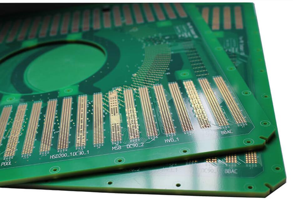
Physically, a multi-processor board is a dense mixed-signal design with several high-speed buses running in parallel. Each processor bus has its own timing budget, and the dual-port memories sit in the middle of two of them, so the layout has to keep the two sides separated and the reference planes continuous under both. This is the same discipline that any high-speed board needs, and the layout rules that keep bus timing predictable are described in our PCB design and layout service.
Power delivery is the second constraint. Several processors drawing current at the same instant produce a load step that the regulator has to answer, and if each processor has its own core rail the sequencing between them has to be defined so that no device is driven before its supply is valid. Splitting the ground plane carelessly between the processors makes the problem worse rather than better, because the return current of a bus that crosses a split has to find a long path around it.
The third point is the boot and debug path. In a loosely coupled system one processor is the boot processor and the others are application processors. The boot processor has to be able to hold the others in reset, initialise the shared region and then release them, which means reset distribution and a small amount of glue logic are part of the architecture rather than an afterthought.
Software Structure
Most systems of this kind run a real-time operating system on every processor, with the same image configured slightly differently for the boot processor and the application processors. The shared memory network is presented to the application as a network interface, so a message between two processors looks like a message over a local network and the application code barely changes.
The boot processor performs the role of shared memory network master. It initialises the shared region, publishes the anchor structure that every other processor uses to find that region, and allocates memory to the processors as they come up. It also keeps a heartbeat counter in the shared memory header, updated every second, so the other processors can tell whether the network is healthy by watching the value change.
Communication itself can be interrupt driven or polled. A polled input queue is simpler and predictable in latency, and it costs processor time at a fixed rate. An interrupt driven queue, using either a bus interrupt or a mailbox interrupt, responds faster and consumes less idle time, and it is the better choice wherever the message rate is bursty.
Resource Allocation Between Processors
Once several processors share one board, the peripheral devices become a resource to be allocated. The simplest approach is static: a device belongs to one processor, fixed at design time, and the other processors reach it through a message. That is easy to verify but inflexible, because a firmware change that moves work between processors also moves the device ownership.
The flexible approach puts the arbitration in programmable logic on the board and leaves a software interface above it, so ownership can be assigned at run time. The hardware must then handle arbitration and priority properly, otherwise two processors can reach a critical resource at the same time. This is the kind of requirement that is best captured while the netlist is still open, which is why an industrial PCBA programme that starts with the schematic review catches it early.
What the Performance Numbers Mean
A measured example is useful because it shows the shape of the result rather than a marketing figure. With a processing algorithm split into modules and distributed across the processors of such a system, two processors improved throughput by roughly sixty to seventy percent over one, and three processors roughly doubled it.
The numbers never scale linearly, and the reason is not the hardware. The split of the algorithm determines how much data has to cross the shared interconnect and how much of the work stays serial. A split that duplicates data in every processor pays for it in communication, and a split that leaves a serial section in one processor caps the gain no matter how many processors are added.
Bringing the Board to Production
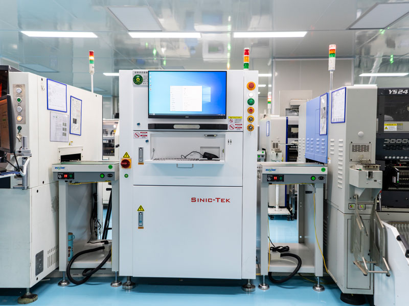
A dense multi-processor board with several fine pitch devices, dual-port memories and a power tree of its own is a manufacturing task as much as a design task. The paste deposit, the placement of the larger processors and the thermal profile all interact on a board of this size, and a small pilot build before volume is the cheapest way to find the interactions.
Testing is the other half. A board with several processors needs a test sequence that powers the rails in order, checks each device independently and then exercises the interconnect, because an interconnect fault and a processor fault look identical from the application. Building that sequence into the fixture, and having the assembly partner report failures per step rather than per board, is what makes the yield improvement loop fast.
FAQ
Does a multi-processor board always need a real-time operating system? No, but most do. A real-time kernel gives each processor its own scheduler and provides the shared memory network module that carries the inter-processor messages.
How should the shared memory connection be treated on the PCB? As two high-speed buses sharing one device. Keep the reference plane continuous under both sides, keep the two buses separated until they meet at the memory, and place the decoupling at the device rather than at the edge of the board.
What failures should the production test catch first? Supply sequencing and the reset distribution, because a board whose rails come up in the wrong order may still appear to pass a functional test before failing intermittently.
For teams planning a design of this class, the practical starting point is a review of the architecture against the process capability of the assembly partner, so the package choices, the layer count and the test access are agreed before the layout is fixed. Our turnkey PCB assembly team works through that review with the design team from the first prototype onward.