Multilayer PCB Impedance Routing for Differential Pairs
Differential pairs carry the high-speed traffic on most multilayer boards. A USB link, a display interface or a serializer lane all depend on two traces behaving as one controlled structure. Impedance routing is the discipline that keeps that structure intact from the driver to the receiver. On a multilayer stackup, the pair is defined by width, spacing, dielectric thickness and the reference plane beneath it. Small process drift in any of these turns into a large yield loss, so the rules belong in layout and fabrication together.
The buyer and the engineer should read the same numbers. Target impedance, tolerance, stackup and critical nets belong in one document before the first panel is built. That document lets the fabricator adjust trace width for etch compensation and lets the assembler keep the pair intact through reflow. Reviewing the routing plan before tooling saves rework later in the run. The sections below set out the placement, routing, stackup and test decisions that decide whether the pair meets its target.
Placement Before Routing
Component placement sets the length of every differential pair on the board. Related devices should sit as close together as practical, because a shorter connection reduces total pair length and cuts unnecessary vias. Placement also decides how many layer transitions the pair must make. Each transition adds parasitic capacitance and inductance, and each one can disturb the impedance. Moving two devices closer during placement is cheaper than fixing a long, via-heavy route later. Engineers should settle placement before detailed routing begins.
High-speed interfaces punish every extra routing segment. A pair that crosses the board to reach a connector picks up skew, crosstalk and reference-plane problems along the way. The placement review should therefore check connector orientation, driver and receiver positions, and the path between them. If the path must change layers, plan the transition point early and keep both traces together. Buyers reviewing a layout should ask where each critical pair starts and ends. That single question exposes most placement problems before fabrication starts.
Parallel and Symmetric Routing
Differential traces should run parallel and stay similar in width along the whole path. Consistent spacing matters as much as consistent width, because coupling between the two traces sets the differential impedance. Sharp 90-degree corners should be avoided on high-speed pairs. Use 45-degree segments or curved traces instead. The two traces should reference the same plane, so one side does not see a different return path from the other. Symmetry is the principle that ties these rules together.
Spacing should follow the impedance target rather than a universal number. A common guideline keeps pair spacing relatively tight and consistent, often near twice the trace width, but the exact value comes from the stackup calculation. Width and spacing are solved together against the dielectric thickness and copper weight. Buyers should check that the layout notes cite the stackup used for that calculation. A pair routed to a generic rule may pass visual review and still miss its target impedance after fabrication.
Series Components and Length Matching
Series resistors and capacitors in a differential path need symmetric placement. Two components in a pair should align vertically or horizontally with each other, so neither trace takes a longer detour. This keeps trace lengths similar, routing geometry consistent and parasitic effects balanced. Asymmetric placement forces one side of the pair around a component while the other runs straight. The result is skew and common-mode conversion. Engineers should check series component orientation during layout review, not after the board is assembled.
Matched length is the next requirement. If one trace is longer than the other, the two signals arrive at different times and differential skew degrades the received signal. The electrical path should be symmetric in trace length, via count, via structure, layer transitions and reference-plane conditions. Visual similarity is not enough. A pair can look balanced and still carry different parasitic loads on each side. Length matching matters most where timing margin is tight, such as high-speed serial interfaces with little budget to spare.
Compensating Mismatch
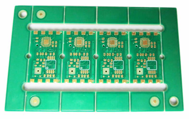
Perfect length matching is not always possible. Pin locations, via positions, routing channels and board space can force one trace longer than the other. When mismatch is significant, compensate as close as practical to where it occurs. A common design target keeps the difference within about 5 mil for sensitive interfaces, though the interface specification and timing budget should set the real limit. Avoid adding large serpentine sections at the end of the route just to force equal nominal length.
Excessive meandering increases coupling between adjacent segments and can harm signal integrity.
Stackup and Impedance Calculation
Trace width alone does not set impedance. A trace over a reference plane behaves differently as the distance to that plane changes. The calculation must consider trace width, spacing, copper thickness, dielectric thickness, dielectric constant, reference-plane location and solder mask thickness together. Impedance calculators such as Polar Instruments Si9000 are common in engineering workflows. The dielectric constant varies with material and construction, so the manufacturer’s material data and stackup should be used whenever available. Generic values are a starting point, not a substitute for real specifications.
Solder mask also shifts impedance, and its effect is easy to overlook. The mask thickness and its dielectric constant belong in the model alongside the copper and core dimensions. Fabricators apply etch compensation, which changes the finished trace width from the drawn width. That adjustment should feed back into the calculation before release. A properly defined stackup makes communication between designer and manufacturer much easier. It also gives the buyer a fixed reference for comparing quotes, because each supplier calculates against the same physical structure.
Common Routing Problems
Several practices create impedance discontinuities on multilayer boards. Excessive vias are the most common, since every layer transition adds capacitance and inductance. Inconsistent spacing changes coupling along the path and shifts differential impedance. Asymmetric routing sends one trace around a via or component while the other runs direct, so the two signals see different electrical environments. Poor reference-plane continuity is another frequent cause.
A split, void or unsuitable layer transition forces return current onto a longer path, which raises radiation and disturbs impedance. Each of these problems is cheaper to fix in layout than in fabrication.
Excessive serpentine compensation deserves its own warning. Length matching is important, but tightly spaced parallel segments of the same trace couple to one another. That coupling raises local capacitance and changes the effective impedance of the pair. Compensation should be designed deliberately, with adequate spacing between meander legs. Engineers should also check that the reference plane stays continuous beneath the meander. A correction that fixes skew while breaking impedance continuity trades one problem for another.
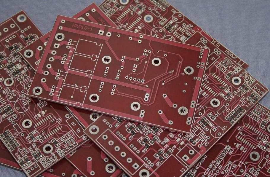
Buyers should ask for the skew budget and the compensation method in the layout review package.
Fabrication and Test Verification
Controlled impedance is not only a layout issue. Manufacturing tolerances affect the final impedance of every board. Final trace width, copper thickness, dielectric thickness, etching compensation, lamination registration, material dielectric constant, solder mask thickness and layer-to-layer alignment all move the result. The designer should send the target impedance, tolerance, stackup, reference layers and critical nets to the manufacturer. A capable fabricator can then verify whether the specified impedance is achievable before production. This review prevents a costly surprise at first article.
After fabrication and assembly, critical high-speed boards may need impedance-related verification depending on the application. For assembled boards, electrical and functional testing help identify defects that could affect system performance. Our PCBA testing covers these checks, and quality management keeps impedance control inside the wider quality system. Coupon measurements, time-domain reflectometry and continuity checks each answer a different question about the pair. Buyers should confirm which method applies to their board and what tolerance the report will show.
What Buyers Should Verify
A short review before release catches most differential pair problems. Confirm that the stackup used in the impedance calculation matches the fabrication drawing. Check that critical pairs keep consistent width and spacing and that both traces reference the same plane. Verify the skew budget and where compensation is applied. Ask how many vias each pair uses and whether the via structure is identical on both sides. Request the fabricator’s etch compensation figures and the material dielectric constant they will use.
For prototype and volume stages, the same questions apply with different weight. Rapid PCBA prototyping lets a team measure real behavior before committing to volume, while high-volume PCB assembly demands that the process hold those numbers across every lot. SMT PCB assembly adds its own constraints, since reflow and handling must not disturb the pair geometry. A supplier that answers these points with data rather than assurances is the safer choice for controlled impedance work.
The practical takeaway is simple. Fix the stackup first, calculate width and spacing from it, then route both traces with symmetry in mind. Keep vias few and identical, compensate skew where it occurs, and keep the reference plane continuous under the whole pair. Send the target impedance and tolerance to the fabricator before tooling, and ask for the measurement method in writing. These steps cost little at the start and protect the schedule when the boards arrive.