PCB Thermal Profiling of Wave: A Practical Review for Manufacturing Teams Modern electronics depend on boards that are assembled correctly the first time. Every product – a phone, a charger, a medical instrument or an industrial controller – relies on thousands of solder joints that must conduct current for years.…
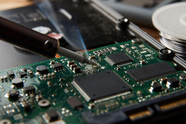
PCB Selective Solder Nozzle Cleaning: A Practical Review for Manufacturing Teams Electronics manufacturing has become a discipline of small details. Solder paste volumes, placement accuracy, temperature profiles and inspection limits all add up to the final result. This guide looks at PCB selective solder nozzle cleaning from the perspective of…
PCB Ion Chromatography Test: What Matters on the Production Line Electronics manufacturing has become a discipline of small details. Solder paste volumes, placement accuracy, temperature profiles and inspection limits all add up to the final result. This guide looks at PCB ion chromatography test from the perspective of a PCBA…
Ceramic PCB Guide: Materials, Processes and Design Rules A ceramic PCB is chosen when the board has to do something an organic laminate cannot: hold a bare die at a controlled temperature, stand off a high voltage at high temperature, or survive a thermal cycle that would fatigue an FR4…
Direct Plated Copper: A Complete Technical Guide Direct plated copper is a process that creates the conductive layer inside a hole without the graphite or the palladium catalyst that a conventional electroless copper line requires. Instead, a conductive polymer is deposited on the dielectric surface and then copper is electroplated…
LED Lighting PCB Basics: Substrate, Thermal Design and Layout An LED luminaire lives or dies by its thermal path, and the printed circuit board is the first link in that path. Unlike a logic board, an LED board feeds a continuous current into devices that turn much of it into…
PCB Workmanship Class 3 Requirements: What Buyers and Engineers Should Check Modern electronics depend on boards that are assembled correctly the first time. Every product – a phone, a charger, a medical instrument or an industrial controller – relies on thousands of solder joints that must conduct current for years.…
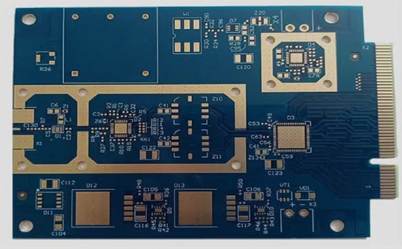
PCB Icicle and Bridging in Wave: Design, Process, and Quality Notes Buyers and engineers often focus on the finished product and forget the production line behind it. In practice, most field failures can be traced back to process decisions made during assembly. Understanding PCB icicle and bridging in wave gives…
PCB Wave Solder Contact Time: Design, Process, and Quality Notes Buyers and engineers often focus on the finished product and forget the production line behind it. In practice, most field failures can be traced back to process decisions made during assembly. Understanding PCB wave solder contact time gives you a…
PCB Workmanship Standard Training: Design, Process, and Quality Notes Electronics manufacturing has become a discipline of small details. Solder paste volumes, placement accuracy, temperature profiles and inspection limits all add up to the final result. This guide looks at PCB workmanship standard training from the perspective of a PCBA factory…