PCB Bed of Nails Probe Wear: From Prototype to Volume Production Buyers and engineers often focus on the finished product and forget the production line behind it. In practice, most field failures can be traced back to process decisions made during assembly. Understanding PCB bed of nails probe wear gives…
PCB Depaneling Stress: From Prototype to Volume Production Modern electronics depend on boards that are assembled correctly the first time. Every product – a phone, a charger, a medical instrument or an industrial controller – relies on thousands of solder joints that must conduct current for years. This article explains…
Phone PCB vs Tablet PCB: What Actually Differs A phone and a tablet run the same operating systems and use similar chipsets, so it is easy to assume their boards are alike. They are not. The constraints that shape each design pull in different directions, and the resulting boards differ…
Space Grade PCB Manufacturing: Reliability Above All Hardware that leaves the atmosphere cannot be repaired, which changes every design decision on the board. A space grade PCB is specified not to perform well on average but to survive every foreseeable condition, and the production discipline that follows is closer to…
PCB Laser Depaneling: Clean Cuts Without Contact Laser depaneling separates finished boards from a panel using a focused beam instead of a rotating blade. The beam removes a narrow path of material and leaves the adjacent circuitry untouched. Because nothing presses on the board, the mechanical stress that worries thin…
OLED Display PCB Cost Factors: Materials, Process and Yield An OLED display PCB is not a large board, but it carries an unusual combination of requirements: a very fine-pitch bonding area for the display driver, a high-speed interface to the host, a thin overall profile and a mechanical outline that…
PCB Fixture Design for Test: A Factory-Floor Review Electronics manufacturing has become a discipline of small details. Solder paste volumes, placement accuracy, temperature profiles and inspection limits all add up to the final result. This guide looks at PCB fixture design for test from the perspective of a PCBA factory…
PCB Floor Life Tracking on the Line: Practical Process Controls Modern electronics depend on boards that are assembled correctly the first time. Every product – a phone, a charger, a medical instrument or an industrial controller – relies on thousands of solder joints that must conduct current for years. This…
AR Device PCB: Design Challenges for Wearable Displays An augmented reality headset is one of the hardest packaging problems in consumer electronics. Two displays have to be driven at high frame rate, several cameras have to be captured and processed, a radio has to work beside all of that, and…
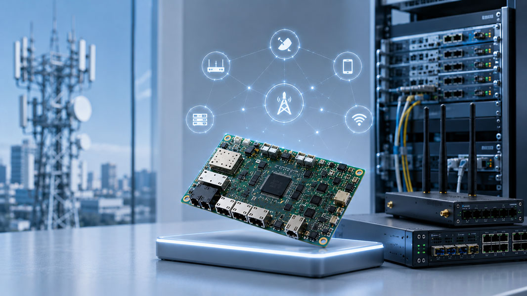
Telecom PCBA: Rugged Design for Continuous Operation A telecom PCBA is designed around a requirement that most consumer boards never face: it has to keep working. Equipment in a base station, an optical node or a switching centre is expected to run continuously for years, at temperature extremes, with no…