OLED Display PCB Cost Factors: Materials, Process and Yield
An OLED display PCB is not a large board, but it carries an unusual combination of requirements: a very fine-pitch bonding area for the display driver, a high-speed interface to the host, a thin overall profile and a mechanical outline that fits a module.
Those requirements push fabrication and assembly into processes that are more demanding than the board size would suggest, and that is why the price per square centimetre is high compared with ordinary control boards.
Why OLED Boards Are Unusual
The electrical interface to a display module is fast, often using a high-speed serial link, while the driver connection is extremely dense. The same board must therefore satisfy high-speed signal integrity and very fine pitch at the same time.
Mechanically, the board is part of a module that includes the panel, a cover glass and a housing. Its thickness, flatness and outline are constrained by the module assembly, and those constraints propagate directly into fabrication requirements.
Fine-Pitch Bonding and Chip on Board
Where the driver is bonded directly to the board, the pad pitch can be below 50 microns. That requires a flat surface, a finish that supports the bonding method and a pad geometry defined by the bonding process rather than by assembly tolerance.
Chip on board assembly uses ultrasonic or thermosonic bonding, and the reliability of the joint depends on the surface finish and cleanliness of the pads. A finish with the wrong hardness or thickness produces weak bonds that fail during thermal cycling.
Fine pitch also raises the inspection requirement. Optical inspection of a 30 micron pitch is marginal, so X-ray or electrical continuity testing is used to verify the bonds.
<img src="https://www.gopcba.com/wp-content/uploads/2020/12/project-image-6.jpg" alt="Thin substrate PCB prepared for a display module” />
Layer Count and Routing Density
The number of signals that must leave a display module is high, and the escape area is limited. Boards of this type often use four to eight layers with fine traces and small vias to route the interface away from the bonding area.
Where the layer count is high relative to the board size, the fabrication cost per unit area rises sharply, because the fixed cost of lamination, drilling and registration is spread over very few square centimetres.
Substrate Thickness and Material
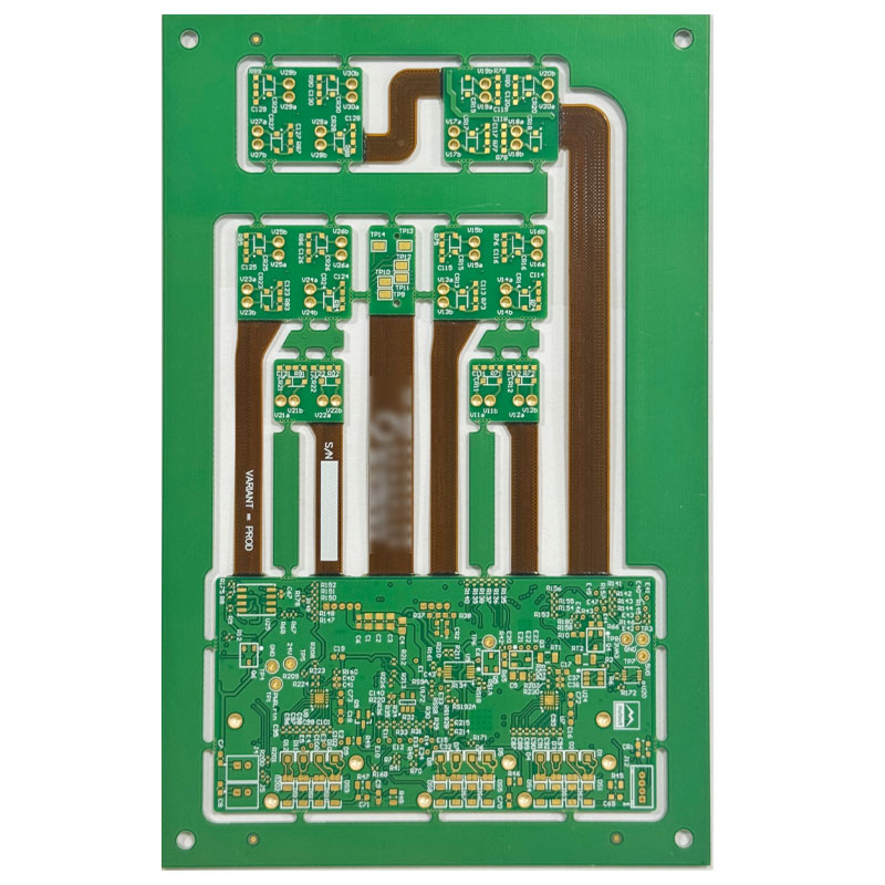
Module thickness limits the board to a thin substrate, often 0.4 to 0.8 millimetres. Thin boards require carriers during processing, and they are more sensitive to warpage and to handling damage.
Where the high-speed interface runs at a rate that standard FR-4 cannot support over the required length, a low-loss material is used. On a small board the material cost is modest compared with the processing cost, so the choice is usually driven by performance rather than by price.
Power and Ground Design
Displays are sensitive to supply noise, which appears as flicker or as uneven brightness. The supply for the driver and the panel should be heavily decoupled, with the capacitors close to the load and a low-impedance plane returning the current.
Ground continuity matters as much as decoupling. A display PCB usually has a continuous ground plane, and any slot under the high-speed interface or under the supply path creates a return current detour that shows up as noise on the panel.
Assembly Constraints
The assembly process must handle a thin board with fine-pitch components on one side and possibly a bonded driver on the other. Panel design, support and handling become critical, and the yield loss from handling can exceed the loss from the bonding process itself.
The display itself is usually attached after the board is assembled. That sequence imposes a flatness requirement on the board, because a warped board makes the panel attachment unreliable and can produce uneven pressure across the display.
Yield and Inspection
Yield is the largest cost item on a display board, because the process is at the edge of capability. Fine traces, small vias, thin substrates and fine-pitch bonding each contribute their own loss, and the losses compound.
Inspection is correspondingly thorough: automated optical inspection for the surface features, electrical test for continuity, and often functional test of the display against the final interface rather than only at the board level.
Where Cost Can Be Reduced
Simplify the stack where the routing allows, and use via-in-pad only where the escape genuinely requires it. Each build-up layer on a small board is a disproportionate cost item.
Standardise the interface. Where a module can use a standard high-speed link instead of a custom parallel bus, the layer count and the routing density both fall, and the board becomes considerably cheaper to build.
Finally, review the panel. A display board is often assembled alongside other boards on a shared panel, and the arrangement determines the tooling cost and the handling risk.
Testing the Module Interface
Testing at the board level is not sufficient for a display module. The electrical behavior of the interface changes once the panel is attached, because the panel adds capacitance and the flex adds length.
Module-level test therefore measures the actual interface, including brightness uniformity, flicker and the eye quality of the high-speed link with the panel connected. Catching a marginal interface at the module stage is far cheaper than finding it after the product is assembled.
Supplier Selection
Display boards are built by a limited set of suppliers, because fine-pitch bonding and thin-substrate handling require specific equipment. The chosen supplier’s process capability defines the design rules that can be used, and those rules should be obtained before the layout starts.
Coupon structures, bonding test vehicles and a first article with a full microsection review are all appropriate on a first order. On a display board, the process is as important as the artwork, and the qualification should reflect that.
Design Checklist
Confirm the bonding pad geometry against the driver manufacturer recommendation, verify the surface finish against the bonding method, check the interface length against the signal integrity budget, and confirm that the board flatness after assembly meets the module requirement.
Then check the mechanical interface: the outline, the mounting features and the position of the connector relative to the display. On a module board, a mechanical error costs more than an electrical one because it affects the panel as well.
Further reading: via in pad versus plated through, microstrip and stripline routing, and FPGA board high-speed interfaces.
Reviewed against the module requirement rather than only the board requirement, a display design is far more likely to pass its first build without a mechanical revision.
Confirm the interface, the bonding geometry and the mechanical outline with the module assembly drawing before release, because those three items are the ones that cannot be corrected by a layout change once tooling exists.
FAQ
Why is a display PCB so expensive per unit area? Because the fixed cost of a high layer count and a thin-substrate process is spread over a very small board, and the yield loss on fine features adds a further premium.
Does the display driver have to be bonded to the board? Not always. Where the driver is supplied on the panel flex, the board only carries the interface, which relaxes the pad pitch and reduces cost considerably.
What causes flicker in a display that works on the bench? Usually return current or decoupling. A plane slot under the supply path or a capacitor placed too far from the driver produces supply variation that appears as visible brightness variation.