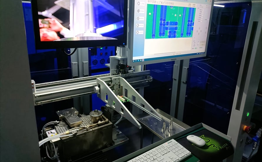
Micro Hole Machining Methods in PCB Production Hole sizes on printed circuit boards have fallen steadily as boards moved from single-sided to multilayer construction and as density increased. The definitions used in production are simple: a diameter below 0.6 mm is a small hole, and one below 0.3 mm is…
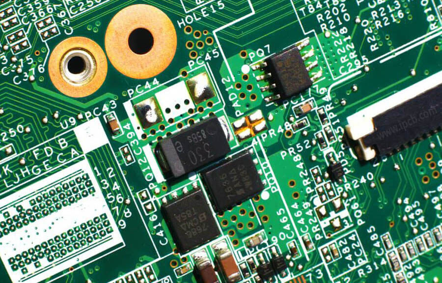
Choosing Pad and Hole Sizes for PCB Prototypes Hole size looks like a trivial dimension. A lead of a known diameter goes into a hole of a slightly larger diameter, and the pad around it is drawn to suit. In practice the choice is constrained from both sides: the hole…
Why High Tg Material Matters in PCB Fabrication Every laminate has a temperature at which its mechanical behaviour changes. Below that point it is rigid and its dimensions are stable. Above it, the resin softens, expands faster and loses the stiffness that the rest of the process depends on. That…
Selecting Copper Thickness for PCB Prototypes Copper thickness is specified in ounces, a unit inherited from the weight of foil used per square foot. One ounce copper is about thirty-five microns thick, and it is the default for most boards. Raising it changes what the board can carry, how it…
PCB Design Layers Explained: Signal, Plane, Mask, and Mechanical Modern layout software presents the design as a stack of named layers, and new engineers often find the number of them overwhelming. Each layer has a specific role, and each one produces a different output file or a different instruction to…
PCB Copper Balancing Across Layers: Practical Process Controls Modern electronics depend on boards that are assembled correctly the first time. Every product – a phone, a charger, a medical instrument or an industrial controller – relies on thousands of solder joints that must conduct current for years. This article explains…
PCB Panel Copper Distribution: Practical Process Controls Buyers and engineers often focus on the finished product and forget the production line behind it. In practice, most field failures can be traced back to process decisions made during assembly. Understanding PCB panel copper distribution gives you a practical advantage when you…
PCB Production Process: Twelve Steps From Data to Final Test A bare board is produced by a sequence of operations where each step depends on the accuracy of the one before it. The PCB production process begins with engineering data and ends with an electrical test, and the yield of…
Metal Core PCB Design and DFM: Stackup, Vias and Grounding Metal core boards are rare in consumer products and everywhere in lighting, power conversion, industrial drives and aerospace equipment. The reason is simple: a high power stage produces heat that has to leave the package quickly, and a glass reinforced…
PCB Etching Quality: Undercut, Etch Factor and Defects PCB etching quality is decided long before the panel reaches the etcher, even though this is the step that finally reveals the circuit pattern. In a pattern plating process, a resist layer is plated onto the copper that must remain and the…