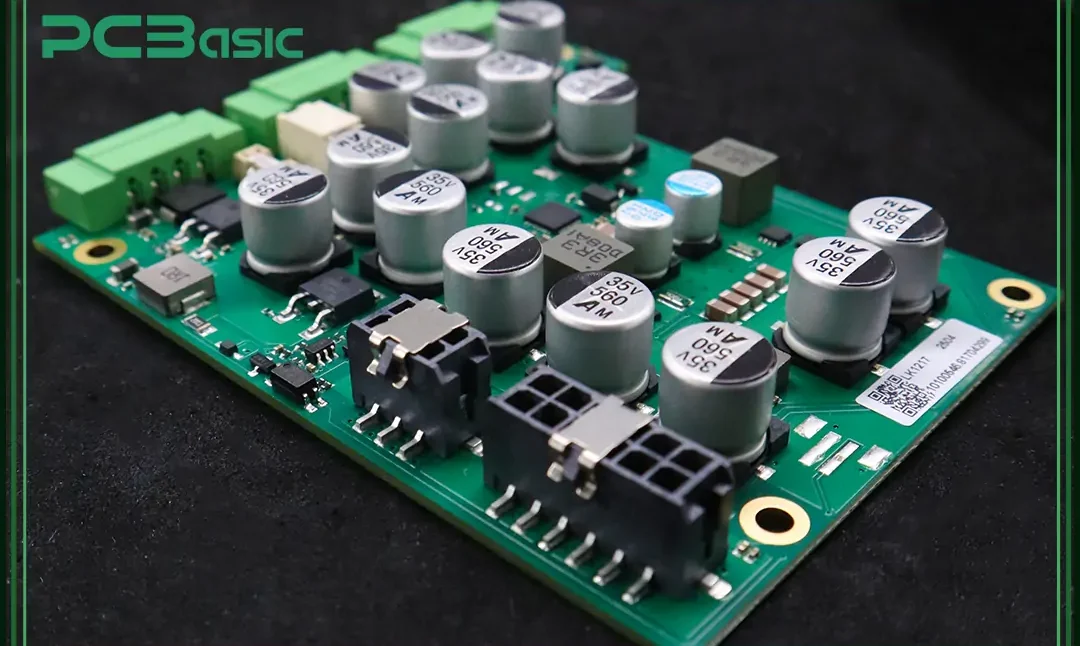
Mixed Signal PCB Design Guidelines Boards that contain both analog and digital circuits are the most common source of difficult layout problems, because the two halves of the design want opposite things. Analog circuitry measures small continuous signals and needs a quiet, stable reference. Digital circuitry switches state abruptly, draws…
Trace Width and Current: Calculating the Right Copper Sizing a trace for current is one of the few layout decisions with a closed-form answer, and it is also one of the most frequently skipped. A trace that is too narrow will heat up, increase its resistance, heat up further, and…
Blind Via and Buried Via Stack Selection A through via is the simplest way to connect two layers, and for most designs it is still the right answer. Choosing between the structures is really a question of how many lamination cycles the complete via stack requires. It is drilled once,…
PCB Any Layer HDI Stackup: From Design to Repeatable Production Electronics manufacturing has become a discipline of small details. Solder paste volumes, placement accuracy, temperature profiles and inspection limits all add up to the final result. This guide looks at PCB any layer HDI stackup from the perspective of a…
DC-DC Converter Layout and Routing Guidelines A switching regulator converts voltage efficiently because it never operates the pass device in its linear region. The cost of that efficiency is a node that switches between the input rail and ground at hundreds of kilohertz to several megahertz, and every trace connected…
PCB Via Filling for Stacked Microvias: Design, Process, and Quality Notes Electronics manufacturing has become a discipline of small details. Solder paste volumes, placement accuracy, temperature profiles and inspection limits all add up to the final result. This guide looks at PCB via filling for stacked microvias from the perspective…
PCB Rework of A Coated Board: Working Through the Film Buyers and engineers often focus on the finished product and forget the production line behind it. In practice, most field failures can be traced back to process decisions made during assembly. Understanding PCB rework of a coated board gives you…
PCB Recoating A Repaired Area: Repairing the Film Buyers and engineers often focus on the finished product and forget the production line behind it. In practice, most field failures can be traced back to process decisions made during assembly. Understanding PCB recoating a repaired area gives you a practical advantage…
PCB Coating Coverage Under Components: Design and Assembly Considerations Electronics manufacturing has become a discipline of small details. Solder paste volumes, placement accuracy, temperature profiles and inspection limits all add up to the final result. This guide looks at PCB coating coverage under components from the perspective of a PCBA…
STM32 Core Board PCB Design: Rules and Layer Planning A microcontroller core board looks simple: one large device, a handful of passives and a connector that breaks out the pins. In practice it is one of the harder boards to lay out well, because the processor is fast, the power…