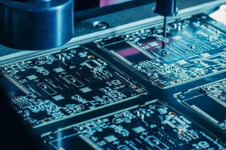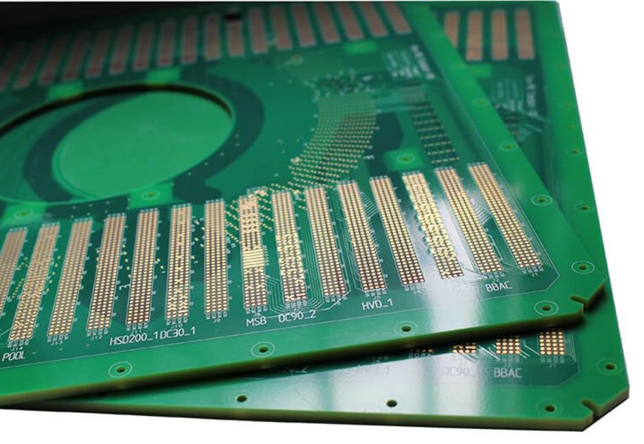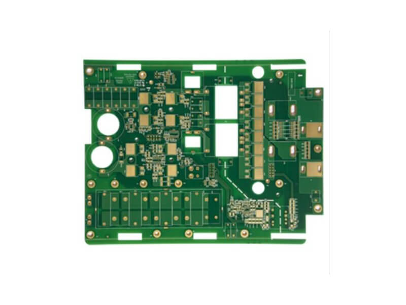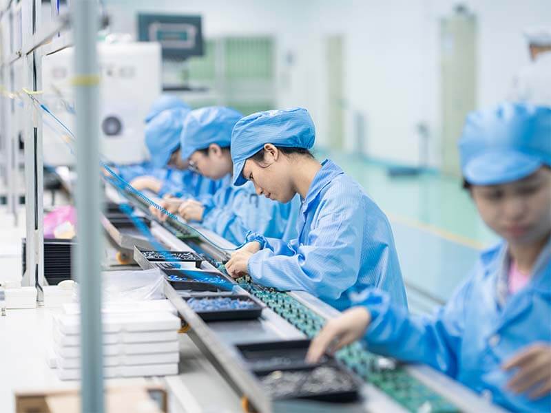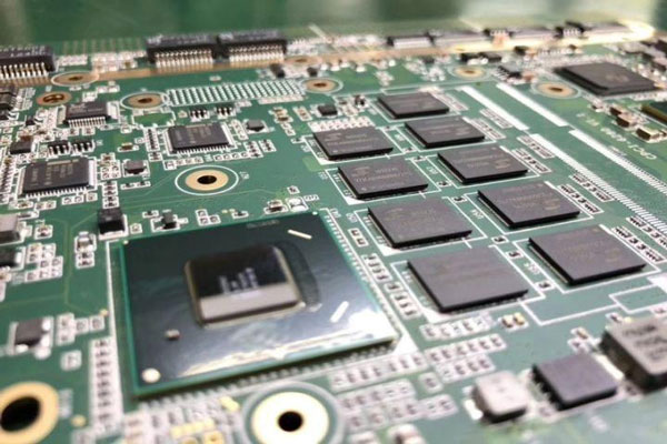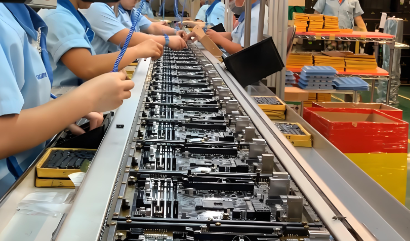
PCB Lead Time Improvement: From Prototype to Volume Production Buyers and engineers often focus on the finished product and forget the production line behind it. In practice, most field failures can be traced back to process decisions made during assembly. Understanding PCB lead time improvement gives you a practical advantage…
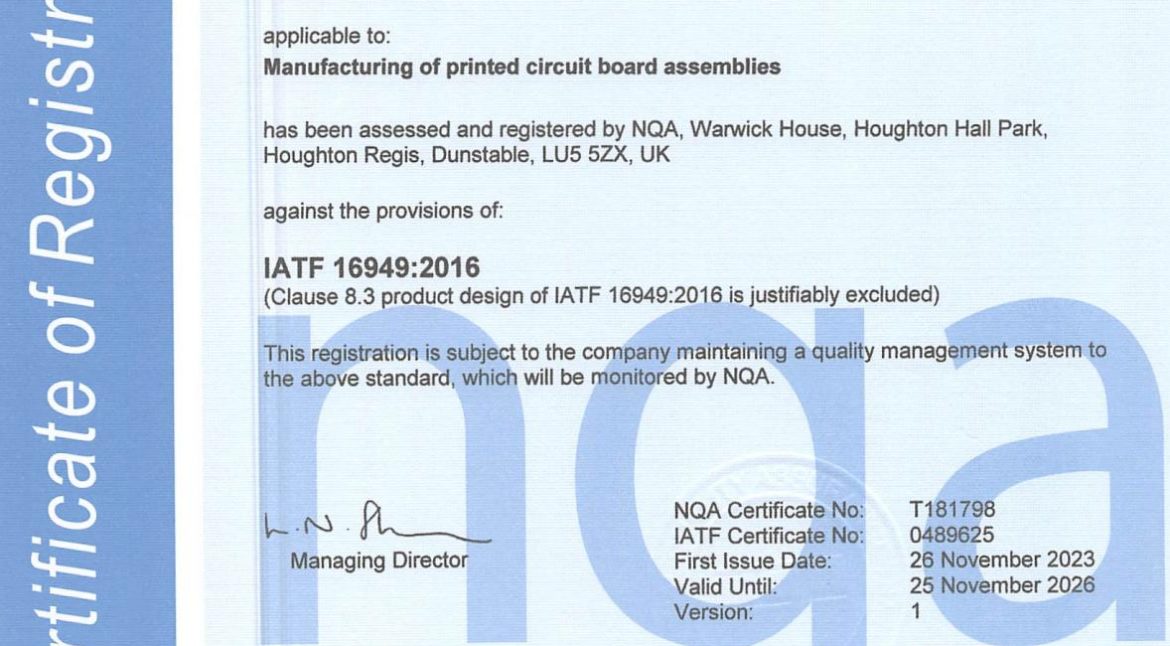
Micro Etch: 5 Rules for Inner Layer Bonding Micro etch is the controlled chemical removal of a thin layer of copper from the surface of a panel before it is treated and laminated. The amount removed is measured in tenths of a micron, and that small cut produces the roughness…
Solder Mask Peeling: 6 Causes and Cures Solder mask peeling is the loss of bond between the coating and the board, and it appears as a lifted edge, a blister or a patch that comes away with a piece of tape. It is found most often after a soldering operation,…
PCB Quotation Review: A Factory-Floor Review Modern electronics depend on boards that are assembled correctly the first time. Every product – a phone, a charger, a medical instrument or an industrial controller – relies on thousands of solder joints that must conduct current for years. This article explains PCB quotation…
Coating Adhesion: 6 Tests Before Release Coating adhesion is what keeps a conformal coating attached to the board for the life of the product, and it is the property most often taken for granted because a freshly coated board looks identical whether the film is bonded or merely resting on…
Acid Copper Plating: 5 Checks on Chloride Level Acid copper plating relies on a small amount of chloride to work, and the quantity involved is small enough that it is easy to lose control of. Chloride is dosed in tens of parts per million, yet the difference between too little…
PCB Quotation Plan: From Design to Repeatable Production Electronics manufacturing has become a discipline of small details. Solder paste volumes, placement accuracy, temperature profiles and inspection limits all add up to the final result. This guide looks at PCB quotation plan from the perspective of a PCBA factory floor, covering…
Press Pad Care: 5 Rules for Even Lamination A press pad is the compliant layer that sits between the press platen and the caul plate, and it is what turns a rigid machine into an even press. Without it, the smallest difference in stack height would be pressed straight into…
PCB Quotation Data: Design, Process, and Quality Notes Modern electronics depend on boards that are assembled correctly the first time. Every product – a phone, a charger, a medical instrument or an industrial controller – relies on thousands of solder joints that must conduct current for years. This article explains…
Resin Flow in Lamination: 5 Checks for a Full Fill Resin flow is the movement of resin out of the prepreg and into the spaces of a multilayer stack during the press cycle, and it is what turns a stack of dry sheets into a solid board. Too little flow…