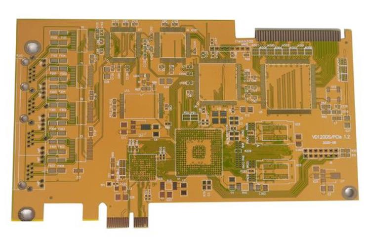
Solder Mask Thickness and Its Effect on Assembly Solder mask is drawn as a two dimensional pattern, but it is printed as a three dimensional layer. Its thickness decides whether the mask can cover a tall trace, whether a dam between two pads survives assembly and whether a via is…

PCB Traceability Selection: Practical Process Controls Buyers and engineers often focus on the finished product and forget the production line behind it. In practice, most field failures can be traced back to process decisions made during assembly. Understanding PCB traceability selection gives you a practical advantage when you choose a…
Panel Utilization: Preparation, Placement and Process Control Printed circuit boards are made on panels and sold as boards, and the difference between the two is where a significant part of the cost lives. Panel utilization is the fraction of the panel that becomes product, and improving it lowers the price…
Thermal Shock Versus Thermal Cycling Tests Thermal shock and thermal cycling both expose a board to a temperature change, and they produce different failures because the rate of change is different. A test that is chosen for the wrong reason qualifies the wrong property. What Separates the Two A thermal…
Solder Joint Grain Structure and Reliability Guide A solder joint is a metal casting on a very small scale, and like any casting it has a grain structure that depends on how it solidified. The grain structure in turn decides how the joint behaves under thermal cycling, how it cracks…
PCB Traceability: Design, Process, and Quality Notes Buyers and engineers often focus on the finished product and forget the production line behind it. In practice, most field failures can be traced back to process decisions made during assembly. Understanding PCB traceability gives you a practical advantage when you choose a…
PCB Traceability Control: Design, Process, and Quality Notes Electronics manufacturing has become a discipline of small details. Solder paste volumes, placement accuracy, temperature profiles and inspection limits all add up to the final result. This guide looks at PCB traceability control from the perspective of a PCBA factory floor, covering…
PCB Traceability Standards: A Practical Manufacturing Guide Electronics manufacturing has become a discipline of small details. Solder paste volumes, placement accuracy, temperature profiles and inspection limits all add up to the final result. This guide looks at PCB traceability standards from the perspective of a PCBA factory floor, covering applying…
Solder Mask Registration on Fine Pitch Pads Solder mask registration is the alignment of the mask openings to the pads, and on a fine pitch design it is the item that decides whether a printable dam exists between two pads. The dam is what holds the paste in place during…
Copper Oxide Treatment for Inner Layer Bonding Inner layer copper is bonded to the resin through a treatment that grows a controlled oxide on the surface. Without it the copper and the resin do not adhere, and with the wrong one the bond is either weak or the oxide is…