Copper Oxide Treatment for Inner Layer Bonding
Inner layer copper is bonded to the resin through a treatment that grows a controlled oxide on the surface. Without it the copper and the resin do not adhere, and with the wrong one the bond is either weak or the oxide is too thick to survive the press.
What the Treatment Does
The treatment converts the surface of the copper into a rough oxide that the resin can key into. The roughness is mechanical and the chemistry is what makes it adhere to both the copper below and the resin above.
The thickness of the oxide is the parameter that matters. Too thin and there is nothing to key into; too thick and the oxide is brittle and separates within itself. Our laminate properties notes describe the resin side of the bond.
Types of Treatment
The brown oxide and the black oxide differ in thickness and in colour, and the black oxide is the thicker of the two. A reduced black oxide is a common compromise, because it keeps the mechanical key while removing the brittle outer layer.
Alternative treatments that do not rely on an oxide are used where the resin chemistry does not bond well to one. Those produce a different surface and require their own process window. Our etching notes describe the surface the treatment is applied to.
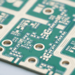
<img src="https://www.gopcba.com/wp-content/uploads/2026/08/Three-green-PCBs-with-diverse-components-prominently-displaying-LED-technology.webp" alt="Treated copper surface before lamination” />
The press applies heat and pressure, and the oxide has to remain intact through both. An oxide that is too thick cracks under the pressure, and one that is chemically unstable dissolves into the resin as the temperature rises.
The result of a failure is a separation between the copper and the resin that appears as a delamination after the assembly reflow rather than at lamination. That is why the treatment is verified by a thermal stress test rather than by appearance.
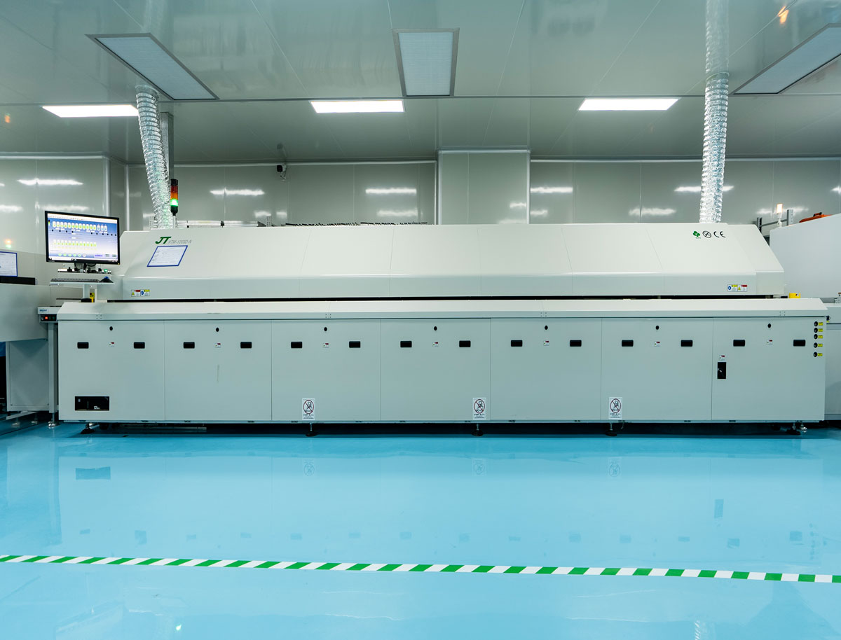
The treated surface is sensitive to handling, and a fingerprint or a scratch on it becomes a bond defect. The panels are handled by the edge, and the queue between the treatment and the press is kept short.
The exposure time matters as well, because the treated surface absorbs moisture and can be damaged by it. A treatment that is left overnight is not the same surface that was produced. Our layer assignment notes describe how that queue is arranged in the flow.
Verification is by peel strength on a sample, by a thermal stress test and by microsection of the interface after lamination. The peel test measures the bond and the section shows where it failed.
The section is the more useful of the two when a failure has occurred, because the failure location distinguishes a treatment problem from a press problem. A bond that fails inside the oxide points at the treatment and one that fails at the resin points at the press. Our board quality notes describe how the result is recorded.
A stack with a large copper area on one layer and a sparse one on another presses unevenly, and the treatment sees a different pressure across the panel. The thieving that balances the plating also balances the press.
That is one reason the copper balance requirement appears in both discussions. It is a plating requirement and it is also a lamination requirement, and the panel is designed once for both.
Process Control and Verification
On a design of this kind, oxide is the item that decides how the rest of the board is arranged. Reviewing the design before the data is released is cheaper than correcting it after the panel is in the tank, because every step downstream inherits the decision made at the front end. Documenting the assumption is part of the design work, and a short note on the drawing prevents a question that would otherwise arrive a day later and cost a day of schedule.
The process window is set by the narrowest step in the flow, so an improvement anywhere else shows up as margin rather than as yield until that step is addressed. A short note on the drawing about handling, storage or packaging is often worth more than an extra decimal place on a tolerance.
Where a value sits close to a process limit, the drawing should say so, since the shop can then open the process window rather than working to a nominal figure that carries no tolerance. A stack-up that is drawn rather than described removes most of the ambiguity from a quotation, and it lets the fabricator price the board against the dielectric and copper weights that will actually be used.
Where the requirement is not written down, the shop supplies its own default, and the default is chosen for the process rather than for the design. The measurements that matter are the repeatable ones: conductor width and spacing, annular ring, finished hole size, plating thickness and surface finish are all verifiable on a coupon that travels with the panel.
Process Control and Verification
On a design of this kind, oxide is the item that decides how the rest of the board is arranged. Reviewing the design before the data is released is cheaper than correcting it after the panel is in the tank, because every step downstream inherits the decision made at the front end. Documenting the assumption is part of the design work, and a short note on the drawing prevents a question that would otherwise arrive a day later and cost a day of schedule.
The process window is set by the narrowest step in the flow, so an improvement anywhere else shows up as margin rather than as yield until that step is addressed. A short note on the drawing about handling, storage or packaging is often worth more than an extra decimal place on a tolerance.
Where a value sits close to a process limit, the drawing should say so, since the shop can then open the process window rather than working to a nominal figure that carries no tolerance.
Process Control and Verification
On a design of this kind, oxide is the item that decides how the rest of the board is arranged. Reviewing the design before the data is released is cheaper than correcting it after the panel is in the tank, because every step downstream inherits the decision made at the front end. Documenting the assumption is part of the design work, and a short note on the drawing prevents a question that would otherwise arrive a day later and cost a day of schedule.
Process Control and Verification
On a design of this kind, oxide is the item that decides how the rest of the board is arranged. Reviewing the design before the data is released is cheaper than correcting it after the panel is in the tank, because every step downstream inherits the decision made at the front end. Documenting the assumption is part of the design work, and a short note on the drawing prevents a question that would otherwise arrive a day later and cost a day of schedule.
Is a darker oxide better? It indicates a thicker one, and thicker is not better because the outer layer is brittle.
Can the treatment be reworked? It can be stripped and re-applied where the panel has not been laminated, and the copper loses a little thickness each time.
What does gopcb provide for inner layer adhesion? We provide a treatment selected for the resin, oxide thickness controlled to a verified range, a short queue between treatment and press, peel and thermal stress tests with sections, handling rules for the treated surface, and records per batch.