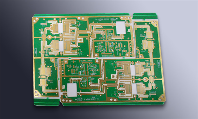
Impedance Coupon Verification for Controlled Boards Impedance coupon verification is the step that proves a controlled impedance stackup is actually being built the way the drawing describes. The board may look correct, the layer count may match and the drill data may be right, yet the trace width, dielectric thickness…

First Pass Yield Improvement on the SMT Line First pass yield is the fraction of units that complete the process without rework, repair or retest. It is the most honest single number a line produces, because it does not care how much effort went into recovering a unit; it only…
Fiducial Design and Machine Vision Alignment Guide A fiducial is a small copper feature that exists only so that a machine vision system can find the board. Without it the placement machine, the paste printer and the automated optical inspection system all have to guess the position from the board…
Cooling Rate and Grain Structure in Lead Free Joints A lead free joint solidifies over a temperature range, and how fast it passes through that range decides the grain structure that forms. The structure is visible in the appearance and measurable in the fatigue life. What the Cooling Rate Controls…
Step Stencils for Mixed Paste Volume Requirements One board usually carries components that want different amounts of paste. A fine pitch device needs a thin deposit to avoid bridging, while a connector on the same board needs a thick one to form a full fillet. A single stencil thickness has…
Laminate Dielectric Constant Measurement Methods Guide The dielectric constant of a laminate is the number that a signal integrity engineer uses to size every trace on a high speed board, so it is worth knowing exactly what a quoted value means. Suppliers quote it on a data sheet, test laboratories…
Copper Weight Selection for PCB Design Copper weight is the thickness of the foil used on a layer, expressed in ounces per square foot. One ounce is about 35 micrometres, and the number decides how much current a trace can carry, how well heat spreads, how finely the copper can…
Packaging Materials as a Source of Contamination A board that has been cleaned can be contaminated again by the material it is packed in. The contamination is invisible, it appears as an adhesion failure or an intermittent contact, and it is found long after the cause has been forgotten. Silicone…
Bake Cycles and Residual Floor Life After Opening A dry packed component has a floor life that starts when the bag is opened. Managing that life across partial reels, part used bags and returns is where most popcorning problems originate. How Residual Life Is Calculated The total floor life comes…
Microsection Preparation and Interpretation A microsection is the only way to see what is actually inside a board or a solder joint. X-ray shows density, electrical test shows continuity, and visual inspection shows the surface, but a polished cross section shows the copper thickness in a barrel, the intermetallic layer…