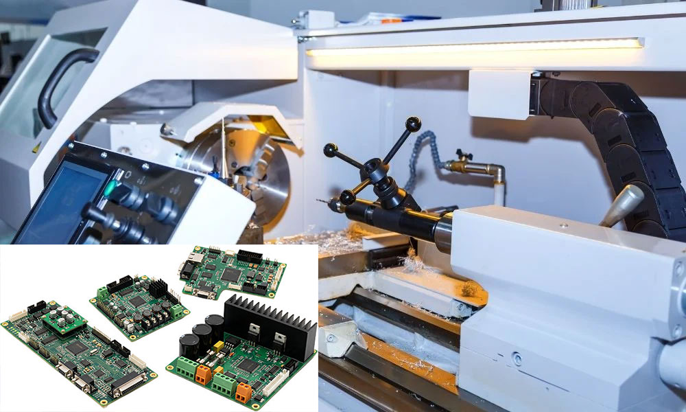
PCB Soldermask Maintenance: A Practical Manufacturing Guide Buyers and engineers often focus on the finished product and forget the production line behind it. In practice, most field failures can be traced back to process decisions made during assembly. Understanding PCB soldermask maintenance gives you a practical advantage when you choose…
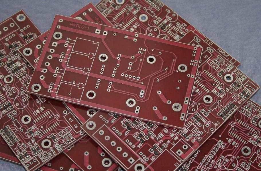
PCB Soldermask Defects: Design, Process, and Quality Notes Electronics manufacturing has become a discipline of small details. Solder paste volumes, placement accuracy, temperature profiles and inspection limits all add up to the final result. This guide looks at PCB soldermask defects from the perspective of a PCBA factory floor, covering…
PCB Soldermask Setup: Design, Process, and Quality Notes Buyers and engineers often focus on the finished product and forget the production line behind it. In practice, most field failures can be traced back to process decisions made during assembly. Understanding PCB soldermask setup gives you a practical advantage when you…
PCB Soldermask Training: Design, Process, and Quality Notes Electronics manufacturing has become a discipline of small details. Solder paste volumes, placement accuracy, temperature profiles and inspection limits all add up to the final result. This guide looks at PCB soldermask training from the perspective of a PCBA factory floor, covering…
SMT Adhesive Dispensing and Cure for Wave Soldering Adhesive holds surface mount components in place while the board passes over a wave of molten solder, and it does the job only if the dots are the right size, in the right place and cured to the right degree. A dot…
PCB Soldermask Records: Process Details and Inspection Points Modern electronics depend on boards that are assembled correctly the first time. Every product – a phone, a charger, a medical instrument or an industrial controller – relies on thousands of solder joints that must conduct current for years. This article explains…
Conductive Anodic Filament Growth In PCB Laminate Conductive anodic filament, usually shortened to CAF, is a failure in which a conductive path grows through the laminate between two conductors held at different potentials. The path follows the interface between the resin and the glass fibre bundle, and once it bridges…
Moisture Absorption: Design Rules and Process Limits Every organic laminate absorbs a small amount of water from the air. The amount is measured as a percentage by weight and it looks trivial, yet the absorbed water changes the electrical and mechanical properties of the material and creates the internal pressure…
PCB Soldermask Checklist: What Matters on the Production Line Modern electronics depend on boards that are assembled correctly the first time. Every product – a phone, a charger, a medical instrument or an industrial controller – relies on thousands of solder joints that must conduct current for years. This article…
PCB Soldermask Audit: What Matters on the Production Line Buyers and engineers often focus on the finished product and forget the production line behind it. In practice, most field failures can be traced back to process decisions made during assembly. Understanding PCB soldermask audit gives you a practical advantage when…