Minimum Line Width Selection For PCB Designs The minimum line width on a board is the narrowest conductor the fabricator can produce reliably on that particular stack, and it is one of the first questions a designer should ask. A value that is too aggressive increases cost and reduces yield,…
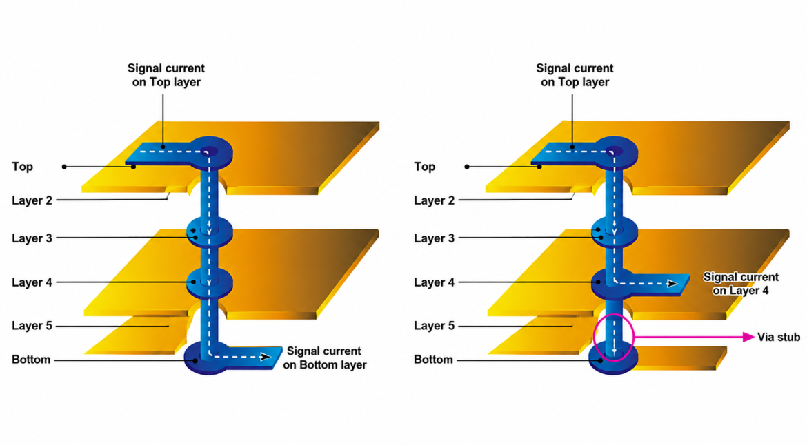
Layer Count Selection For Multilayer Boards Layer count is the first structural decision in a multilayer design, and it drives almost everything that follows: the stackup, the board thickness, the impedance options, the via structure and the price. It is also one of the decisions most often made too early,…
PCB Copper Plating Cost: A Factory-Floor Review Buyers and engineers often focus on the finished product and forget the production line behind it. In practice, most field failures can be traced back to process decisions made during assembly. Understanding PCB copper plating cost gives you a practical advantage when you…
PCB Copper Plating Training: Key Process and Quality Checks Buyers and engineers often focus on the finished product and forget the production line behind it. In practice, most field failures can be traced back to process decisions made during assembly. Understanding PCB copper plating training gives you a practical advantage…
PCB Copper Plating Audit: Checking the Practice Buyers and engineers often focus on the finished product and forget the production line behind it. In practice, most field failures can be traced back to process decisions made during assembly. Understanding PCB copper plating audit gives you a practical advantage when you…
Stencil Design Rules for SMT Printing A stencil is a thin metal foil with apertures cut to match the pads, and it is the tool that decides how much paste reaches each pad. The printing process has little room to correct a stencil that is wrong, so the stencil design…
PCB Copper Plating Checklist: A Factory-Floor Review Modern electronics depend on boards that are assembled correctly the first time. Every product – a phone, a charger, a medical instrument or an industrial controller – relies on thousands of solder joints that must conduct current for years. This article explains PCB…
PCB Copper Plating Records: A Factory-Floor Review Electronics manufacturing has become a discipline of small details. Solder paste volumes, placement accuracy, temperature profiles and inspection limits all add up to the final result. This guide looks at PCB copper plating records from the perspective of a PCBA factory floor, covering…
PCB Copper Plating Problems: From Design to Repeatable Production Buyers and engineers often focus on the finished product and forget the production line behind it. In practice, most field failures can be traced back to process decisions made during assembly. Understanding PCB copper plating problems gives you a practical advantage…
Solder Paste Thawing: Design Rules and Process Limits Solder paste is a mixture of solder powder, flux and a solvent system, and its behaviour changes with temperature and with time. Most printing problems that are blamed on the printer or the stencil can be traced to paste that was used…