Layer Count Selection For Multilayer Boards
Layer count is the first structural decision in a multilayer design, and it drives almost everything that follows: the stackup, the board thickness, the impedance options, the via structure and the price. It is also one of the decisions most often made too early, from a rough impression rather than from an estimate.
The choice can be approached in a structured way. Routing density and the number of plane layers set a lower bound, signal integrity sets constraints on the arrangement, and cost and lead time push the answer upward until it settles on a standard build.
Why Layer Count Is A Design Decision
Each added layer gives one more routing plane, but it also adds two more interfaces, more lamination steps and more opportunities for misregistration. The added cost is not just material: handling, drilling and inspection all scale with the layer count, and the yield on a twenty layer board is much lower than on a four layer board.
Because the decision constrains everything downstream, changing it late is expensive. A design that has been routed for six layers cannot simply be moved to eight without redoing the planes, and a design that was assumed to fit on four may prove impossible once the high speed nets are considered.
Routing Density And The First Estimate
A useful starting estimate is to count the signal nets crossing a typical section and compare that with the tracks that fit per layer. A low cost board uses 100 to 150 microns of width and spacing, giving roughly one track per millimetre of usable width per layer, and that figure falls quickly as the rules tighten.
The estimate should be based on the densest region rather than the average, because the dense area is what forces the layer count up. Adding a layer for the average and then finding that a small area cannot be routed is one of the common ways a design slips past its planned schedule.
Plane Layers And Reference
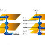
Planes are not only power distribution; they are the reference for every controlled impedance trace and for every high speed signal. A design with two plane layers can reference signals on both sides of the pair, while a design with a single plane can only provide a good return path for the traces adjacent to it.
As the number of planes grows, the arrangement matters more than the count. A stackup that places two plane layers far apart loses the benefit of the second one for high frequency return currents, while one that places them either side of a signal layer gives that layer a clean reference on both faces. The way power is distributed across those planes is described under power plane splitting rules.
Signal Integrity And The Stackup
Signal integrity requirements usually add layers rather than remove them, because a controlled impedance trace needs a reference plane at a defined distance. When the required impedance cannot be reached with the available dielectric thickness, the answer is often to change the stackup rather than the trace geometry.

High speed interfaces such as DDR memory or a differential serial link also need a reference plane that is continuous under the whole route. That requirement alone can force an additional plane layer, even though the routing itself would fit on fewer. The routing rules behind these constraints are described under multilayer PCB advantages for high speed.
Cost And Lead Time
Cost rises with layer count in steps rather than smoothly, because fabricators build standard constructions and price around them. Moving from four to six layers is a smaller jump than moving from six to eight, and a non-standard odd count is usually more expensive than the next even count above it.
Lead time behaves in the same way. Standard constructions are held in stock and can be built quickly, while a custom stackup requires foil and prepreg to be ordered in. For a prototype, choosing a standard construction can save a week even when the layer count is one higher than the minimum. The stackup itself is described under layer stackup from one to eight layers.
Reaching The Decision
A practical sequence is to estimate the routing requirement, add the plane layers the interfaces demand, then round up to the next standard construction and check the cost. If the price is unacceptable, the routing rules can be tightened before the layer count is reduced, because that trade is cheaper to reverse.
The decision and its justification should be recorded, since it explains many later constraints. How the stackup is documented for the fabricator is described under PCB design and fabrication.
Process Control and Verification
On a design of this kind, layer count is the item that decides how the rest of the board is arranged. A stack-up that is drawn rather than described removes most of the ambiguity from a quotation, and it lets the fabricator price the board against the dielectric and copper weights that will actually be used. Where the requirement is not written down, the shop supplies its own default, and the default is chosen for the process rather than for the design.
The measurements that matter are the repeatable ones: conductor width and spacing, annular ring, finished hole size, plating thickness and surface finish are all verifiable on a coupon that travels with the panel. Running a first article through the same checks as the production panel confirms that the two agree, and that comparison is the cheapest form of process control available at prototype stage.
Keeping a sample from the panel turns a dispute into a measurement, because the same coupon can be re-examined by both parties without rebuilding the batch.
Process Control and Verification
On a design of this kind, layer count is the item that decides how the rest of the board is arranged. A stack-up that is drawn rather than described removes most of the ambiguity from a quotation, and it lets the fabricator price the board against the dielectric and copper weights that will actually be used. Where the requirement is not written down, the shop supplies its own default, and the default is chosen for the process rather than for the design.
The measurements that matter are the repeatable ones: conductor width and spacing, annular ring, finished hole size, plating thickness and surface finish are all verifiable on a coupon that travels with the panel.
Process Control and Verification
On a design of this kind, layer count is the item that decides how the rest of the board is arranged. A stack-up that is drawn rather than described removes most of the ambiguity from a quotation, and it lets the fabricator price the board against the dielectric and copper weights that will actually be used. Where the requirement is not written down, the shop supplies its own default, and the default is chosen for the process rather than for the design.
A first article check confirms that the process and the drawing agree on the points listed above, and that the coupon data supports the values used in the design.
Where a measurement falls outside the expected window, the sample is retained so that the cause can be established before the balance of the batch is released.
FAQ
Should an odd layer count ever be used? It can be, but odd counts are often built as the next even number with a dummy layer, so the saving is small. An odd count is worth considering mainly when the thickness is tightly constrained.
How many plane layers does a design need? At least one for a simple board, and two for anything with controlled impedance or a high speed interface, so that signals can be referenced on both sides of a plane pair.
Can the layer count be reduced by using finer lines? Sometimes, but the saving in layers is often outweighed by the higher cost of the fine line process and by the loss of current capacity. Price both options before deciding.