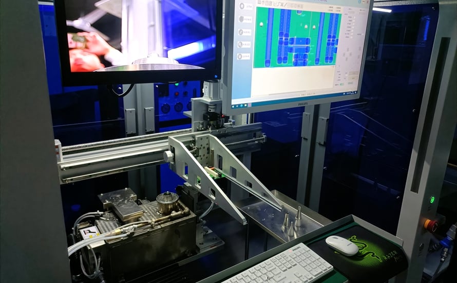
PCB SPI Plan: Laying It Out First: A Practical Manufacturing Guide Buyers and engineers often focus on the finished product and forget the production line behind it. In practice, most field failures can be traced back to process decisions made during assembly. Understanding PCB SPI plan gives you a practical…
Dielectric Constant Measurement Methods for Laminates The dielectric constant of a laminate determines how fast a signal travels in a trace and how wide the trace has to be to present a given impedance. It is the number a designer uses most often when a controlled impedance stack is designed,…
PCB SPI Data: What the Numbers Say: Design, Process, and Quality Notes Buyers and engineers often focus on the finished product and forget the production line behind it. In practice, most field failures can be traced back to process decisions made during assembly. Understanding PCB SPI data gives you a…
UV Laser Depaneling For Assemblies Laser depaneling separates boards from their panel with a focused beam instead of a router bit. It applies no mechanical force to the assembly, it can follow any outline including a curve or an internal cut-out, and it leaves no dust in the sense of…
Package On Package Stacking Design A package on package assembly places one packaged device on top of another, with the two joined by a perimeter array of solder balls that carries the signals between them. The arrangement is used where a logic device and a memory device have to be…
PCB SPI Limits: Where the Edges Are: A Practical Manufacturing Guide Buyers and engineers often focus on the finished product and forget the production line behind it. In practice, most field failures can be traced back to process decisions made during assembly. Understanding PCB SPI limits gives you a practical…
PCB SPI Setup: Getting Ready for Production Solder paste inspection catches print problems before components hide them. That sounds simple until a line changeover arrives. The program, the stencil, the paste and the operator all shift at once. Getting ready means settling each of those items before the first board…
Via Tenting: Design Rules and Process Limits Solder mask over a via can be applied in two quite different ways. Tenting covers the via completely, with the mask bridging across the drilled hole and sealing it. Plugging fills the hole with mask ink or with a dedicated plugging material, leaving…
CTE Measurement Methods for PCB Laminate Selection Copper expands about five times as much as the laminate around it, so a plated hole in a printed circuit board is under stress every time the board changes temperature. The coefficient of thermal expansion describes how much a material grows for each…
PCB SPI Maintenance: Key Process and Quality Checks Electronics manufacturing has become a discipline of small details. Solder paste volumes, placement accuracy, temperature profiles and inspection limits all add up to the final result. This guide looks at PCB SPI maintenance from the perspective of a PCBA factory floor, covering…