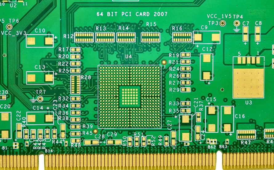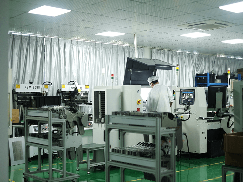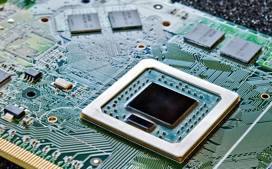
PCB Reel Change Procedure: From Prototype to Volume Production Electronics manufacturing has become a discipline of small details. Solder paste volumes, placement accuracy, temperature profiles and inspection limits all add up to the final result. This guide looks at PCB reel change procedure from the perspective of a PCBA factory…
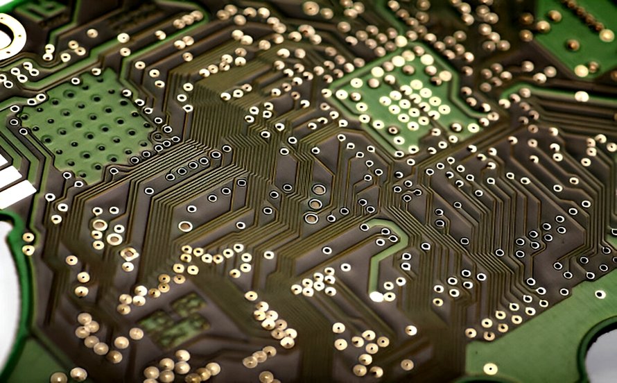
EDX Analysis and SEM Imaging in PCB Failure Analysis Failures rarely announce their own cause. A pad that lifts after reflow, a joint that cracks in the field, a residue that corrodes a trace months after shipment — each of these leaves chemical fingerprints behind. When a board fails, the…
Repair Strategy: Levels of Repair and Spares Planning How far a repair goes depends on where it is performed and on what the repaired unit must subsequently be trusted to do. A repair at the production line and a repair in a service centre are different operations with different requirements.…
PCB Paste Expiry Control: Practical Process Controls Modern electronics depend on boards that are assembled correctly the first time. Every product – a phone, a charger, a medical instrument or an industrial controller – relies on thousands of solder joints that must conduct current for years. This article explains PCB…
PCB Step Stencil Design: A Factory-Floor Review Electronics manufacturing has become a discipline of small details. Solder paste volumes, placement accuracy, temperature profiles and inspection limits all add up to the final result. This guide looks at PCB step stencil design from the perspective of a PCBA factory floor, covering…
Field Returns: Diagnosis and Failure Classification A returned unit is the only evidence about how the product behaves in the field. Handling it as a repair job rather than as an investigation wastes the information it carries. The Return Process Begins Before the Unit Arrives The information accompanying the unit…
PCB Missing Component Detection: From Design to Repeatable Production Buyers and engineers often focus on the finished product and forget the production line behind it. In practice, most field failures can be traced back to process decisions made during assembly. Understanding PCB missing component detection gives you a practical advantage…
Depaneling Methods Compared: Router, Laser and Punch Most boards are built as part of a panel so that the assembly equipment has something to handle, and at some point that panel has to be divided into single boards. How it is divided decides how much mechanical stress reaches the solder…
PCB Bridging Defect: Joined When They Should Not Be A bridge is a solder joint that reaches a neighbor it was never meant to touch. On a fine pitch board, that extra metal can short two signals or hide under a component body. The defect rarely comes from one bad…
Wearable Device PCB Design: Materials and Antennas A wearable is a radio, a battery, a sensor and a processor inside something the size of a wristband, and the board has to survive being worn. There is no established standard for that combination, so the design decisions come from the physics…