PCB Control Chart Selection: Key Process and Quality Checks Modern electronics depend on boards that are assembled correctly the first time. Every product – a phone, a charger, a medical instrument or an industrial controller – relies on thousands of solder joints that must conduct current for years. This article…
Return Path Continuity and Reference Plane Splits A signal leaves its driver and returns to its receiver through a conductor that the schematic does not show. Where that return path is not continuous, the signal finds another route, and the change in the loop area is what produces the emissions,…
Stack-up Planning: Layers, Dielectric Thickness and Cost The stack-up is the decision that determines the impedance, the routing capacity, the cost and the fabrication yield of a board. It is usually made early, often by default, and revisited only when something has gone wrong. What the Stack-up Determines The number…
PCB Ion Chromatography Testing: A Factory-Floor Review Electronics manufacturing has become a discipline of small details. Solder paste volumes, placement accuracy, temperature profiles and inspection limits all add up to the final result. This guide looks at PCB ion chromatography testing from the perspective of a PCBA factory floor, covering…
PCB Sampling Plan Design: Practical Process Controls Electronics manufacturing has become a discipline of small details. Solder paste volumes, placement accuracy, temperature profiles and inspection limits all add up to the final result. This guide looks at PCB sampling plan design from the perspective of a PCBA factory floor, covering…
PCB AQL Levels Explained: From Design to Repeatable Production Buyers and engineers often focus on the finished product and forget the production line behind it. In practice, most field failures can be traced back to process decisions made during assembly. Understanding PCB AQL levels explained gives you a practical advantage…
Solder Preforms and Step Soldering for Thermal Budgets Solder preforms are pieces of solder formed into a defined shape and volume, used where the joint needs more material than a paste deposit can provide or where the alloy has to melt at a temperature the rest of the assembly cannot…
PCB Defect Classification: Design, Process, and Quality Notes Modern electronics depend on boards that are assembled correctly the first time. Every product – a phone, a charger, a medical instrument or an industrial controller – relies on thousands of solder joints that must conduct current for years. This article explains…
PCB Material Review Board: Design, Process, and Quality Notes Modern electronics depend on boards that are assembled correctly the first time. Every product – a phone, a charger, a medical instrument or an industrial controller – relies on thousands of solder joints that must conduct current for years. This article…
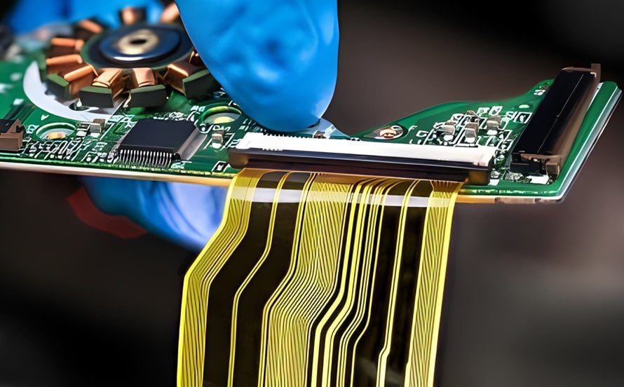
PCB Continuity Test Method: Design and Assembly Considerations Electronics manufacturing has become a discipline of small details. Solder paste volumes, placement accuracy, temperature profiles and inspection limits all add up to the final result. This guide looks at PCB continuity test method from the perspective of a PCBA factory floor,…