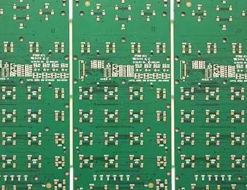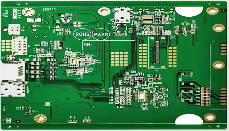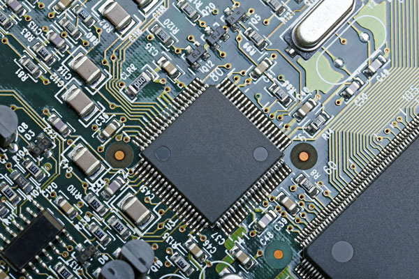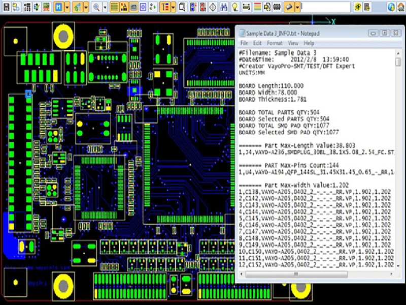
Fiber Weave Effect: Why Differential Pairs Drift A differential pair is supposed to be two traces that see identical conditions, so that any disturbance affects both of them equally and cancels at the receiver. On a real board that assumption is not quite true, because the laminate underneath is not…
Hall Effect Sensor Interface Design A Hall effect sensor converts a magnetic field into an electrical signal without contact, which makes it the natural choice for position, speed and current measurement in equipment that has to run for years. The device itself is simple, but the interface around it decides…
Solder Mask Bridges and the LDI Process A solder mask bridge is the narrow strip of mask that remains between two adjacent pads after imaging and development. Its purpose is to stop solder from bridging the pads during reflow, which makes it a functional feature rather than a cosmetic one.…
PCB PA Matching Network: Design, Process, and Quality Notes Buyers and engineers often focus on the finished product and forget the production line behind it. In practice, most field failures can be traced back to process decisions made during assembly. Understanding PCB PA matching network gives you a practical advantage…
PCB RF Shielding Between Stages: A Wall in the Signal Path A shield wall between RF stages is a physical barrier built into the board. It separates a sensitive receive chain from a noisy transmitter, or keeps a local oscillator from leaking into an adjacent amplifier. The wall only works…
PCB Microstrip Design: Design and Assembly Considerations Buyers and engineers often focus on the finished product and forget the production line behind it. In practice, most field failures can be traced back to process decisions made during assembly. Understanding PCB microstrip design gives you a practical advantage when you choose…
PCB Attenuator Design: A Practical Manufacturing Guide Modern electronics depend on boards that are assembled correctly the first time. Every product – a phone, a charger, a medical instrument or an industrial controller – relies on thousands of solder joints that must conduct current for years. This article explains PCB…
PCB Design Pitfalls: Footprints, Clearance, Thermal and Testability Most board problems that reach production are not exotic. They are the same short list of mistakes, repeated across companies and across products, and almost all of them are avoidable with a review process that looks for them deliberately. A layout that…
Moisture Sensitivity Level: Design Rules and Process Limits A reel of components that has been open on the shop floor for a week is not the same material it was when the seal was broken. The plastic package has absorbed moisture from the air, and when the assembly enters reflow…
PCB Power Amplifier Thermal: A Practical Review for Manufacturing Teams Modern electronics depend on boards that are assembled correctly the first time. Every product – a phone, a charger, a medical instrument or an industrial controller – relies on thousands of solder joints that must conduct current for years. This…