KingdaKingdaKingda

Call Us 24/7

+86-181-2376-9076

Send Us Mail

sales@gopcba.com

Our Location

Baoan District, Shenzhen, China

Language

  • enEnglish
    • fr France
    • itItalian
Kingda
  • Home
  • PCB Assembly
    • Prototype PCB Assembly
    • Turnkey PCB Assembly
    • Low Volume PCB Assembly
    • High Volume PCB Assembly
    • SMT PCB Assembly
    • Through Hole PCB Assembly
    • Mixed Technology PCB Assembly
    • Flex PCB Assembly
  • Services
    • PCB Design/Layout
    • PCB Manufacturing
    • Rapid PCBA Prototyping
    • Components Procurement
    • Conformal Coating
    • PCBA Testing
    • Box Build Assembly
    • Wire & Cable Harness Assembly
  • Industry Solutions
    • Medical PCBA
    • Telecommunications PCBA
    • Energy PCBA
    • Industrial PCBA
    • Artificial Intelligence PCBA
    • IOT PCBA
  • Resources
    • PCB Capabilities
    • PCBA Capabilities
    • FAQ
    • Blog
  • About Us
    • About Us
    • Why Us
    • Quality Management
    • Our PCB Assembly Process
  • Contact Us
Get A Quote
Layer up Lamination

IoT Device PCB Assembly: A Step by Step Guide

  • By Frank guo
  • 2026年 9月 13日
  • PCB Assembly
  • No Comments
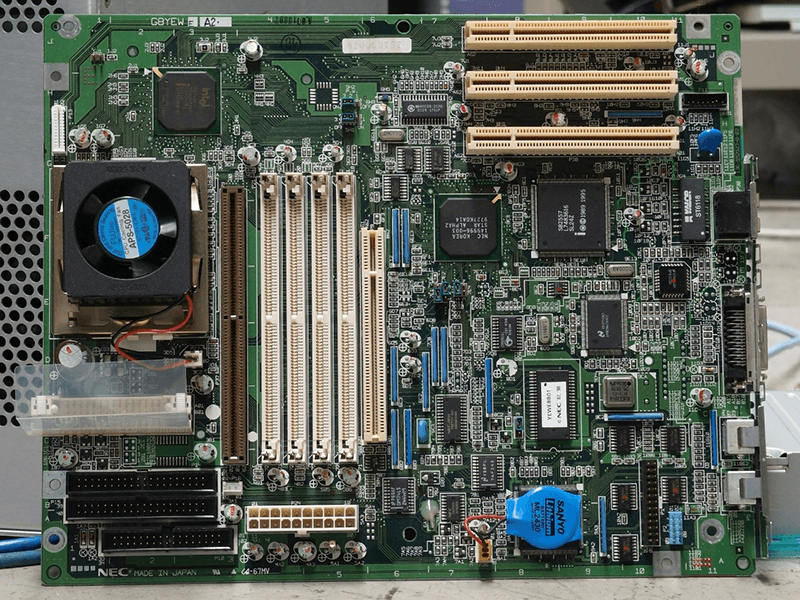
IoT Device PCB Assembly: A Step by Step Guide An IoT device usually has to do several things at once: sense something, process the data, transmit it, and survive for years on a small battery in an environment nobody controls. Each of those requirements leaves a mark on the IoT…
Continue Reading
tupian4

Copper Thickness and Via Plating in Multilayer PCB Fabrication

  • By Frank guo
  • 2026年 9月 13日
  • PCB Assembly
  • No Comments
Copper Thickness and Via Plating in Multilayer PCB Fabrication A multilayer PCB is not a two layer board with more layers. The extra layers bring plated holes with a higher aspect ratio, inner layer copper that has to survive lamination, and impedance requirements that only hold if the whole process…
Continue Reading
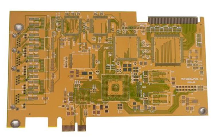
金手指pcb

Parallel PCB Design Flow for Dense High Speed Boards

  • By Frank guo
  • 2026年 9月 13日
  • PCB Assembly
  • No Comments
Parallel PCB Design Flow for Dense High Speed Boards For a long time a printed circuit board could be designed in isolation. A circuit engineer finished a schematic, handed it over, and a layout engineer routed it before passing a data package to the fabricator. Each stage worked from the…
Continue Reading
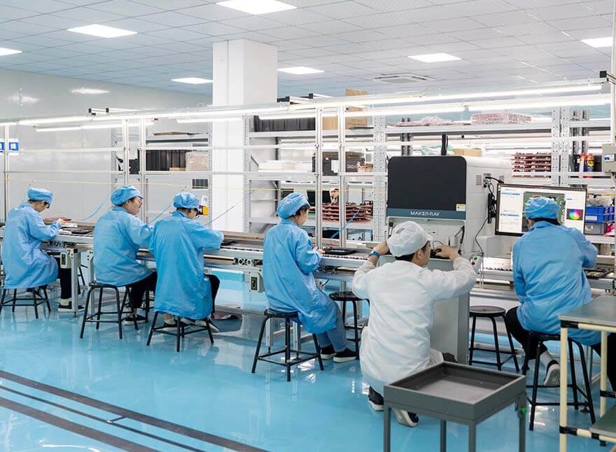
Our DIP Team at Work

From Design Rules to DRC: A Practical PCB Workflow

  • By Frank guo
  • 2026年 9月 13日
  • PCB Assembly
  • No Comments
From Design Rules to DRC: A Practical PCB Workflow A layout tool will let a designer start drawing immediately, and that is the fastest way to produce a board that has to be reworked. The work that prevents rework happens in a fixed order at the beginning: the rules are…
Continue Reading
Vacuum level gauge and seal groove on a drilling chuck

Signal Integrity in the PCB Design Flow

  • By Frank guo
  • 2026年 9月 13日
  • PCB Assembly
  • No Comments
Signal Integrity in the PCB Design Flow Signal integrity is not a property that can be added to a layout at the end. The decisions that decide it, which layer each signal runs on, what it is referenced to, and how far it runs beside its neighbours, are all taken…
Continue Reading
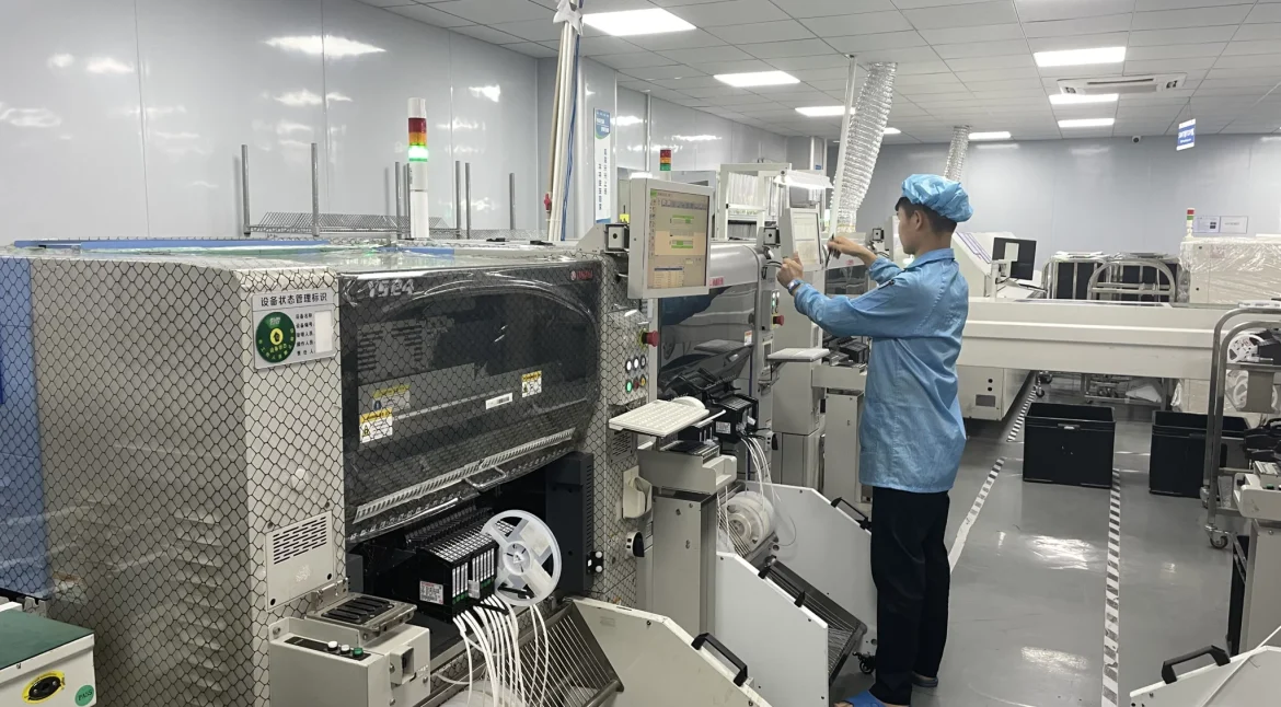
SMT Team in Action

ESP32 PCB Design: Layers, RF Layout and Antenna Clearance

  • By Frank guo
  • 2026年 9月 13日
  • PCB Assembly
  • No Comments
ESP32 PCB Design: Layers, RF Layout and Antenna Clearance A board built around an ESP32 looks simple in the block diagram and behaves very differently in the layout. It carries a radio, a fast digital core and a switch mode supply on a board that is often smaller than a…
Continue Reading
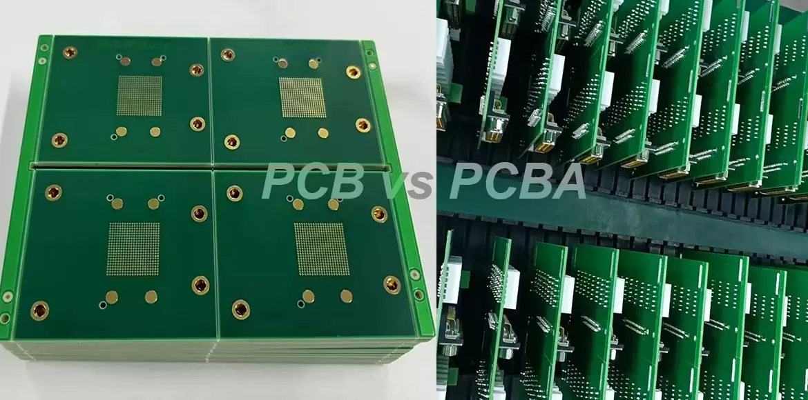
PCB vs PCBA

IoT PCB Copper Thickness: Choosing 0.5 oz or 2 oz

  • By Frank guo
  • 2026年 9月 13日
  • PCB Assembly
  • No Comments
IoT PCB Copper Thickness: Choosing 0.5 oz or 2 oz Copper thickness is the parameter that quietly sets how much current a board can carry, how well it sheds heat and how much it costs, and on a small IoT board it is decided almost by accident. The designer chooses…
Continue Reading
f67cc2b7e36fc7927cc10ee07b9359c-2048×1536

Standard 2-Layer PCB Thickness: 0.8, 1.0 and 1.6 mm

  • By Frank guo
  • 2026年 9月 13日
  • PCB Assembly
  • No Comments
Standard 2-Layer PCB Thickness: 0.8, 1.0 and 1.6 mm Thickness is one of the first numbers a buyer fixes and one of the last to be reconsidered, even though it drives mechanical stiffness, thermal behaviour, impedance geometry and price at the same time. On a two layer board the choice…
Continue Reading
Industrial Automation PCB Assembly

PCB Manufacturing Defects: Causes and Prevention

  • By Frank guo
  • 2026年 9月 13日
  • PCB Assembly
  • No Comments
PCB Manufacturing Defects: Causes and Prevention Every fabrication process has failure modes, and the useful thing about PCB manufacturing defects is that almost all of them are predictable. They cluster around a small number of physical mechanisms, they are visible under the right inspection, and they respond to specific process…
Continue Reading
Quick Turn PCB

BGA Soldering: Voids, Reflow Profile and Inspection

  • By Frank guo
  • 2026年 9月 13日
  • PCB Assembly
  • No Comments
BGA Soldering: Voids, Reflow Profile and Inspection BGA soldering is the point at which the package stops being a part you can inspect with your eyes and becomes a set of joints you have to trust. The balls are underneath the body, the pitch is fine, and the process window…
Continue Reading
1 … 944 945 946 … 1,621

Search Posts

Categories

  • Electronic Materials
  • Electronical Engineering
  • Industrial Control
  • PCB Assembly
  • PCB Design
  • PCB Manufacturing

Recent Posts

Low-Temperature Solder for LED Modules: Thermal Budget and Joint Reliability

Frank guo - 2026年 11月 6日
Surface Mount Technology (SMT): Process, Components, Design Guidelines & PCB Assembly

Surface Mount Technology (SMT): Process, Components, Design Guidelines & PCB Assembly

Zane Zhang - 2026年 10月 2日
Cheap PCB Costs: PCB Design, PCB Manufacturing & SMT vs TH Guide

Cheap PCB Costs: PCB Design, PCB Manufacturing & SMT vs TH Guide

Jelly - 2026年 9月 30日

Tags

AOI inspection automotive electronics automotive PCBA quality automotive standards box build assembly component procurement component supplier conformal coating defect prevention DFM checks DFM review e-bom management electronic component shortage electronic manufacturing services electronic manufacturing standards Electronic Materials electronics design best practice electronics manufacturing capacity electronics sourcing high volume production industrial electronics manufacturability review mass production quality mixed technology PCB PCBA inspection PCBA prototype PCBA turnkey PCBA volume pricing PCB Design PCB layout rules PCB Manufacturing PCB sourcing power electronics PCB printed circuit board prototype quick turn PCB reflow soldering reflow soldering profile SMT assembly quality SMT production soldering defect analysis solder joint quality solder paste inspection solder paste printing surface mount technology vehicle electronics
GOPCBA-logo

As a professional China PCB assembly manufacturer, we provide a full range of electronic manufacturing services from PCB fabrication, PCBA to OEM/ODM, including PCB design, PCB layout, rapid PCBA prototyping, components procurement, SMT/ THT assembly, china pcb assembly, china pcb prototype, PCBA testing and box build assembly.

Linkedin Facebook-f X-twitter Youtube Instagram

PCB ASSEMBLY

  • Prototype PCB Assembly
  • Low Volume PCB Assembly
  • High Volume PCB Assembly
  • Turnkey PCB Assembly
  • SMT PCB Assembly
  • Through Hole PCB Assembly
  • Mixed Technology PCB Assembly
  • Flex PCB Assembly

OUR SERVICES

  • PCB Design/Layout
  • PCB Manufacturing
  • Rapid PCBA Prototyping
  • Components Procurement
  • Conformal Coating
  • PCBA Testing
  • Box Build Assembly
  • Wire & Cable Harness Assembly

TECHNICAL SUPPORT

  • About Us
  • Quality Management
  • Artificial Intelligence PCBA
  • Industrial PCBA
  • IOT PCBA
  • Medical PCBA
  • Energy PCBA
  • Telecommunications PCBA

Copyright © 2026. Shenzhen Kingda Electronics Co., LTD  All rights reserved. 

  • Sitemap
  • Terms of Service
  • Privacy Policy
Zmdi Zmdi-email Phone-square Whatsapp Weixin
x

ABOUT US

Progressively maintain extensive infomediaries via extensible nich. Capitalize on low hanging fruit. a ballpark value added is activity to beta test. Override the digital divide with additional click throughs from fruit.

LOCATIONS

map

Shenzhen Office

+86-181-2376-9076
sales@gopcba.com
3rd Floor, Building 11, Houting Third Industrial Zone, Shajing Avenue, Baoan District, Shenzhen, China.
Contact Us

FOLLOW US