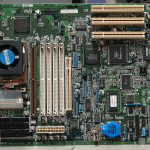
Parallel PCB Design Flow for Dense High Speed Boards
For a long time a printed circuit board could be designed in isolation. A circuit engineer finished a schematic, handed it over, and a layout engineer routed it before passing a data package to the fabricator. Each stage worked from the output of the one before it, and the handovers were where information was lost. That flow still works for a simple board. For a dense board with large area array packages, high speed differential links and tight timing, it produces rework in proportion to how much was decided without the next stage in the room.
Why the Serial Flow Breaks Down
The failure is structural rather than personal. A decision taken at the concept stage – the package, the layer count, the bus architecture – sets constraints that cannot be resolved later. When the layout engineer receives those constraints as a finished decision, the only options left are to work around them or to send the design back, and sending it back costs a delay measured in weeks rather than hours.
A parallel PCB design flow removes the handover as a boundary. The circuit designer and the layout engineer work from the same evolving database, so the consequences of a choice become visible while the choice is still cheap to change. That is the whole benefit, and it is why the tool set has to support shared data rather than a sequence of file transfers.
The Concept Phase
The concept phase is where a parallel flow earns its keep, because it is where the expensive decisions are taken. The questions to settle there are few and consequential: which devices will be used, what packages they come in and how many pins those packages have, how many layers the board will need given the cost and performance trade, and what the target clock frequency and signalling speed will be.
Alongside those sit the architecture choices that layout cannot fix later. Whether a bus is parallel or serial, whether a link needs controlled impedance, and how many power rails the board will carry all determine the stack-up and the routing budget. Impedance mismatch produces reflections and ringing, and no amount of careful routing removes it once the stack-up and the termination scheme are fixed. Settling those questions on paper is the purpose of the phase.

Library, Symbols and the Netlist
Design creation begins with parts. Once the devices are chosen, each one needs a symbol for the schematic and a footprint for the layout, and the two have to agree pin for pin. A footprint error is not caught by any amount of analysis, because the analysis works from the netlist and the netlist is derived from the symbol.
Building the parts first, and checking each footprint against the datasheet drawing, is therefore not overhead. It is the step that makes fast schematic entry possible, because a designer who trusts the library can move parts in and out of a design without re-checking the footprint every time. The same step produces the physical outline and pin arrangement of the large programmable devices, which is where a pin assignment can be adjusted to make the layout easier before anything is routed. The discipline behind the finished data package is described in PCB design and fabrication.
Constraint Capture
Constraints are the rules the layout has to satisfy, and they are captured at the same time as the schematic rather than written afterwards. A design that needs controlled impedance on a bus, length matching within a group, a minimum spacing between a switching node and a sensitive input, or a keep-out under an antenna is a design whose routing rules have to be defined before routing begins.
The trap is over-constraining. A rule set that forbids everything which might conceivably be harmful produces a board that cannot be routed, or a router that satisfies the letter of a rule and misses its intent. The better discipline is to constrain what the analysis shows matters and to leave the rest to normal good practice. Which of those rules come from the fabrication process rather than from the electrical requirement is discussed in PCB design constraints for manufacturing.
Simulation in the Loop
Simulation in a parallel flow is not there to replace prototypes. It is there to avoid building the same prototype several times, because it can find the problems that would otherwise wait until the board is assembled and tested. Running it after the layout is complete means every finding costs a change to routed work.
Run during the flow, the same analysis is cheap. Signal integrity checks on a critical bus can be repeated as the routing evolves, and power integrity can be assessed while the decoupling placement is still being decided. Each iteration is a small correction rather than a design change, and the result is a first article that is more likely to work.

The tool choice follows from that. Two engineers working in the same database see each other’s changes immediately, while two engineers exchanging files see the state of the design only at the moment of exchange. Where the teams sit in different locations the difference is larger rather than smaller, because the cost of a handover is not the file transfer alone but the conversation that has to happen around it, and a conversation held a day later is a day of work built on a superseded decision.
Layout, Review and Handover
Layout is where a parallel flow has to stay parallel. Placement is not an isolated task: the decisions about where a power supply sits, which way a connector faces and how a high speed bus enters the board are made jointly, because each one constrains the others. Placing first and routing later, with no review until the routing is complete, reproduces the serial flow inside a single stage.
Review works the same way. A design review held when the placement is fixed and the critical nets are routed catches problems while they are still local to a region. A review held at the end of the layout catches the same problems as changes to finished work. The practices that shorten the layout stage without shortening the review are described in multilayer design rules to shorten layout, and the way layout choices propagate into production are set out in how PCB layout decisions affect production.
Handover is the last step, and it only works if the data package is complete. The artwork, the drill file, the stack-up with the material and copper weight for every layer, the impedance requirements with the coupon locations, the solder mask and surface finish specification, and the panelisation preference all have to travel together. A package missing one of those items stops at the fabricator as a question, and the question costs the same delay that the parallel flow was meant to remove.
FAQ
What is the main benefit of a parallel design flow? Decisions are made while they are still cheap to change, because the electrical and layout engineers work from one evolving database instead of exchanging finished files.
Which questions belong in the concept phase? The devices and their packages, the layer count, the bus architecture, the target speeds and the impedance strategy. Each of them constrains the stack-up and is difficult to revisit later.
Does simulation replace the first prototype? No. It reduces the number of prototype iterations by finding problems that would otherwise wait until the board is assembled and tested.
What should the data package contain? Artwork, drill data, the stack-up with material and copper weight, the impedance requirements and coupon locations, the solder mask and finish specification, and the panelisation preference.