KingdaKingdaKingda

Call Us 24/7

+86-181-2376-9076

Send Us Mail

sales@gopcba.com

Our Location

Baoan District, Shenzhen, China

Language

  • enEnglish
    • fr France
    • itItalian
Kingda
  • Home
  • PCB Assembly
    • Prototype PCB Assembly
    • Turnkey PCB Assembly
    • Low Volume PCB Assembly
    • High Volume PCB Assembly
    • SMT PCB Assembly
    • Through Hole PCB Assembly
    • Mixed Technology PCB Assembly
    • Flex PCB Assembly
  • Services
    • PCB Design/Layout
    • PCB Manufacturing
    • Rapid PCBA Prototyping
    • Components Procurement
    • Conformal Coating
    • PCBA Testing
    • Box Build Assembly
    • Wire & Cable Harness Assembly
  • Industry Solutions
    • Medical PCBA
    • Telecommunications PCBA
    • Energy PCBA
    • Industrial PCBA
    • Artificial Intelligence PCBA
    • IOT PCBA
  • Resources
    • PCB Capabilities
    • PCBA Capabilities
    • FAQ
    • Blog
  • About Us
    • About Us
    • Why Us
    • Quality Management
    • Our PCB Assembly Process
  • Contact Us
Get A Quote
PCB_Assembly_Process

PCB Sensor Calibration on Board: Trimming in Place

  • By 杰夫
  • 2026年 9月 13日
  • PCB Assembly
  • No Comments
PCB Sensor Calibration on Board: A Practical Manufacturing Guide Electronics manufacturing has become a discipline of small details. Solder paste volumes, placement accuracy, temperature profiles and inspection limits all add up to the final result. This guide looks at PCB sensor calibration on board from the perspective of a PCBA…
Continue Reading
Placement offset before and after self alignment on a reflowed PCB

PCB LED ESD Damage: A Dark Spot on the Line

  • By 杰夫
  • 2026年 9月 13日
  • PCB Assembly
  • No Comments
PCB LED ESD Damage: A Practical Manufacturing Guide Electronics manufacturing has become a discipline of small details. Solder paste volumes, placement accuracy, temperature profiles and inspection limits all add up to the final result. This guide looks at PCB LED ESD damage from the perspective of a PCBA factory floor,…
Continue Reading
One-Stop PCBA Services

PCB LED String Layout: Wiring a Line of Emitters

  • By 杰夫
  • 2026年 9月 13日
  • PCB Assembly
  • No Comments
PCB LED String Layout: A Practical Manufacturing Guide Buyers and engineers often focus on the finished product and forget the production line behind it. In practice, most field failures can be traced back to process decisions made during assembly. Understanding PCB LED string layout gives you a practical advantage when…
Continue Reading
tupian8

PCB Silkscreen Design: Line Width, Clearance and Marking

  • By Frank guo
  • 2026年 9月 13日
  • PCB Assembly
  • No Comments
PCB Silkscreen Design: Line Width, Clearance and Marking Silkscreen is the layer of the design that people read. It identifies the components, marks the orientation of the parts that can be fitted the wrong way, warns about handling restrictions and carries the identifiers that link a board to its documentation.…
Continue Reading
Artificial-Intelligence-Electronics

PCB Trace Width and Current: How to Size Conductors

  • By Frank guo
  • 2026年 9月 13日
  • PCB Assembly
  • No Comments
PCB Trace Width and Current: How to Size Conductors Sizing a conductor is one of the few calculations in board design that can be done on the back of an envelope, and one of the few that is routinely done badly. The physics is simple: a trace has a cross-sectional…
Continue Reading
PCB_test

PCB Board Thickness: Standard Values and Tolerances

  • By Frank guo
  • 2026年 9月 13日
  • PCB Assembly
  • No Comments
PCB Board Thickness: Standard Values and Tolerances Board thickness looks like the simplest parameter in a fabrication drawing and it is one of the most frequently misunderstood. A nominal figure such as 1.6 mm describes a finished board, including the copper and the plating, and the laminate that is ordered…
Continue Reading
microsection of a plated through hole wall

Solder Mask and Paste Mask: Openings, Dams and Stencil

  • By Frank guo
  • 2026年 9月 13日
  • PCB Assembly
  • No Comments
Solder Mask and Paste Mask: Openings, Dams and Stencil Two layers in a circuit board drawing are routinely confused. The solder mask is the permanent coating on the finished board, and the paste mask is a drawing of the openings in the stencil that deposits solder paste during assembly. They…
Continue Reading
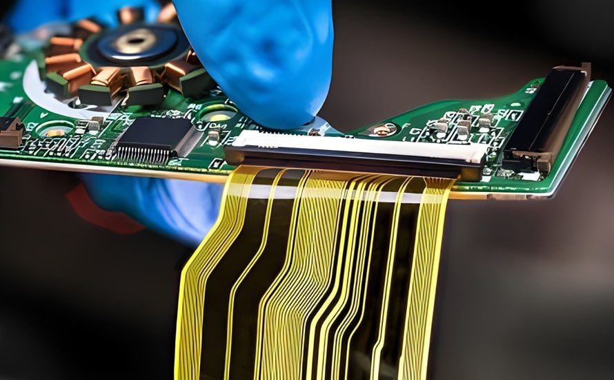
Flex PCB Assembly

PCB Reverse Engineering: How the Process Actually Works

  • By Frank guo
  • 2026年 9月 13日
  • PCB Assembly
  • No Comments
PCB Reverse Engineering: How the Process Actually Works Reverse engineering a board starts from the finished object and works backwards to a schematic. It is used to document equipment that has no available drawings, to reproduce a board whose manufacturer no longer supports it, and to understand how a competitor…
Continue Reading
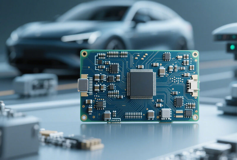
Automotive-PCB-Assembly

PCB Warpage: Bow, Twist and Stackup Balance

  • By Frank guo
  • 2026年 9月 13日
  • PCB Assembly
  • No Comments
PCB Warpage: Bow, Twist and Stackup Balance Warpage is the permanent deformation of a board that should be flat. It appears as a bow along one axis, as a twist across the diagonal, or as a local hump over a copper heavy area, and it shows up at the worst…
Continue Reading
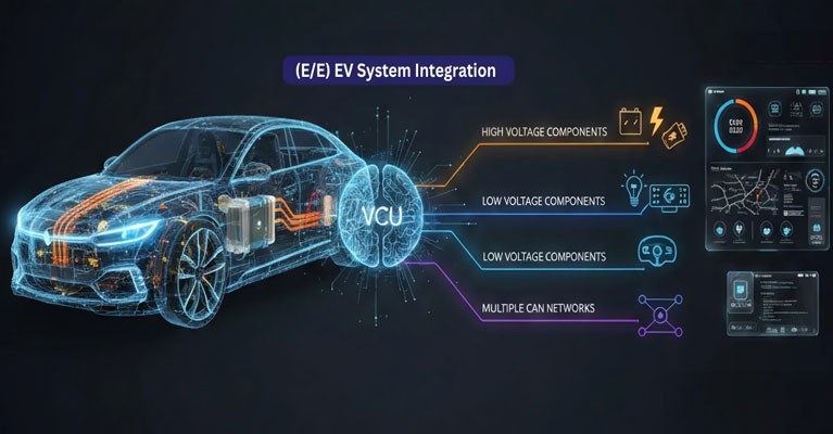
EV-System-Integration

Plated Slot vs Non-Plated Slot in PCB Design

  • By Frank guo
  • 2026年 9月 13日
  • PCB Assembly
  • No Comments
Plated Slot vs Non-Plated Slot in PCB Design Not every hole in a board is round, and not every elongated opening is meant to carry current. A slot can be metallised so that it connects layers and carries a heavy current, or left as bare laminate so that it only…
Continue Reading
1 … 968 969 970 … 1,621

Search Posts

Categories

  • Electronic Materials
  • Electronical Engineering
  • Industrial Control
  • PCB Assembly
  • PCB Design
  • PCB Manufacturing

Recent Posts

Low-Temperature Solder for LED Modules: Thermal Budget and Joint Reliability

Frank guo - 2026年 11月 6日
Surface Mount Technology (SMT): Process, Components, Design Guidelines & PCB Assembly

Surface Mount Technology (SMT): Process, Components, Design Guidelines & PCB Assembly

Zane Zhang - 2026年 10月 2日
Cheap PCB Costs: PCB Design, PCB Manufacturing & SMT vs TH Guide

Cheap PCB Costs: PCB Design, PCB Manufacturing & SMT vs TH Guide

Jelly - 2026年 9月 30日

Tags

AOI inspection automotive electronics automotive PCBA quality automotive standards box build assembly component procurement component supplier conformal coating defect prevention DFM checks DFM review e-bom management electronic component shortage electronic manufacturing services electronic manufacturing standards Electronic Materials electronics design best practice electronics manufacturing capacity electronics sourcing high volume production industrial electronics manufacturability review mass production quality mixed technology PCB PCBA inspection PCBA prototype PCBA turnkey PCBA volume pricing PCB Design PCB layout rules PCB Manufacturing PCB sourcing power electronics PCB printed circuit board prototype quick turn PCB reflow soldering reflow soldering profile SMT assembly quality SMT production soldering defect analysis solder joint quality solder paste inspection solder paste printing surface mount technology vehicle electronics
GOPCBA-logo

As a professional China PCB assembly manufacturer, we provide a full range of electronic manufacturing services from PCB fabrication, PCBA to OEM/ODM, including PCB design, PCB layout, rapid PCBA prototyping, components procurement, SMT/ THT assembly, china pcb assembly, china pcb prototype, PCBA testing and box build assembly.

Linkedin Facebook-f X-twitter Youtube Instagram

PCB ASSEMBLY

  • Prototype PCB Assembly
  • Low Volume PCB Assembly
  • High Volume PCB Assembly
  • Turnkey PCB Assembly
  • SMT PCB Assembly
  • Through Hole PCB Assembly
  • Mixed Technology PCB Assembly
  • Flex PCB Assembly

OUR SERVICES

  • PCB Design/Layout
  • PCB Manufacturing
  • Rapid PCBA Prototyping
  • Components Procurement
  • Conformal Coating
  • PCBA Testing
  • Box Build Assembly
  • Wire & Cable Harness Assembly

TECHNICAL SUPPORT

  • About Us
  • Quality Management
  • Artificial Intelligence PCBA
  • Industrial PCBA
  • IOT PCBA
  • Medical PCBA
  • Energy PCBA
  • Telecommunications PCBA

Copyright © 2026. Shenzhen Kingda Electronics Co., LTD  All rights reserved. 

  • Sitemap
  • Terms of Service
  • Privacy Policy
Zmdi Zmdi-email Phone-square Whatsapp Weixin
x

ABOUT US

Progressively maintain extensive infomediaries via extensible nich. Capitalize on low hanging fruit. a ballpark value added is activity to beta test. Override the digital divide with additional click throughs from fruit.

LOCATIONS

map

Shenzhen Office

+86-181-2376-9076
sales@gopcba.com
3rd Floor, Building 11, Houting Third Industrial Zone, Shajing Avenue, Baoan District, Shenzhen, China.
Contact Us

FOLLOW US