PCB Trace Width and Current: How to Size Conductors
Sizing a conductor is one of the few calculations in board design that can be done on the back of an envelope, and one of the few that is routinely done badly. The physics is simple: a trace has a cross-sectional area, that area determines its resistance, and the resistance together with the current determines how much the trace heats up. Everything else is bookkeeping.
Start With the Copper Cross-Section
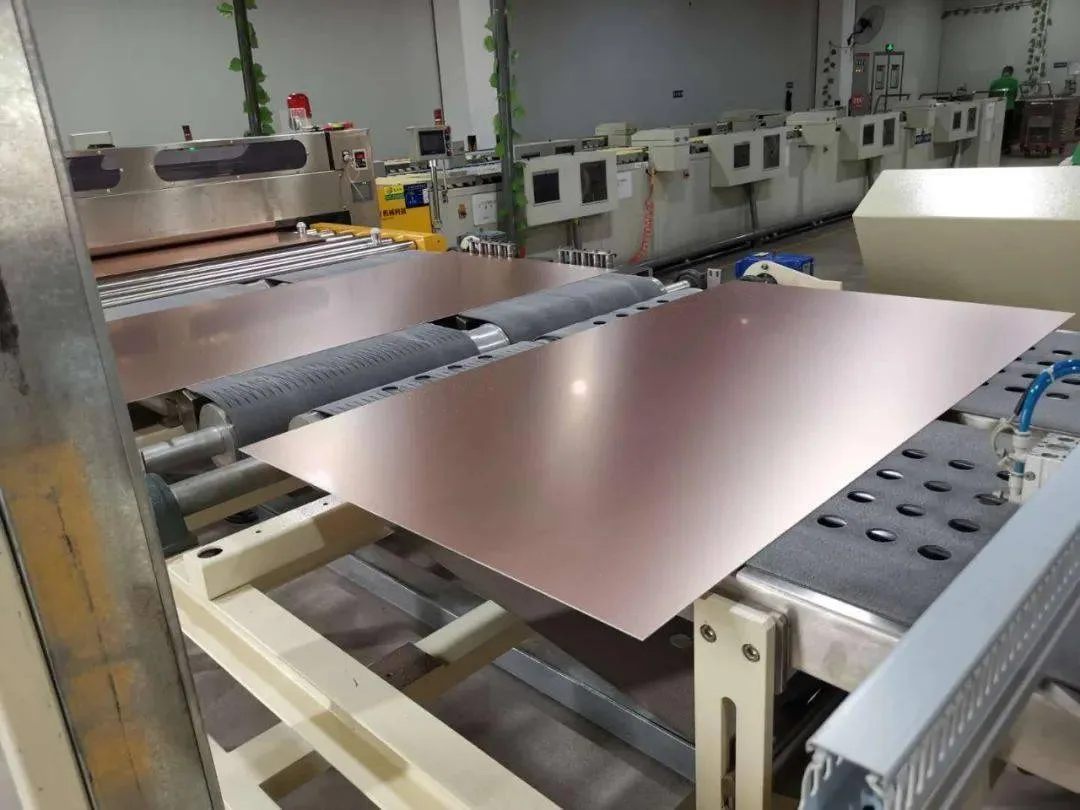
The cross-section of a trace is its width multiplied by the thickness of the copper foil. Most boards use 35 micrometres of copper, which corresponds to one ounce per square foot, so a trace of one millimetre width has a cross-section of about 0.035 square millimetres. The connection between the two is easy to get wrong because the units change twice: the width is normally specified in millimetres or mils and the cross-section in square millimetres or square mils.
Carrying the calculation in consistent units from the beginning avoids most errors. It also makes the effect of the two variables visible: doubling the width doubles the cross-section, while moving from one ounce to two ounces of copper doubles the thickness and therefore the cross-section at the same width.
The Current Density Rule of Thumb
A practical starting point is a current density of between fifteen and twenty-five ampères per square millimetre of copper. Multiply the cross-section by the density and the result is the current the trace can carry. The rule is convenient because it needs no calculator and it gives an answer that is conservative for a trace in still air on an outer layer.
Its weakness is that it ignores temperature rise, which is the quantity that actually matters. A trace carrying its rated current at an acceptable temperature rise is a good design; a trace carrying the same current but reaching an unacceptable temperature is not, even though the density rule gives the same number for both. Density is the shortcut, temperature rise is the specification.
The Temperature-Rise Relationship
The widely used empirical relationship relates the allowable current to the temperature rise and the cross-sectional area. In it, current is proportional to the cross-sectional area raised to roughly the power of three quarters, multiplied by the temperature rise raised to roughly the power of 0.44, with a coefficient that depends on whether the trace is on an inner layer or an outer layer. The inner-layer coefficient is about half the outer-layer value, which reflects the fact that an internal trace cannot dissipate heat into the air in the same way.
Two consequences follow immediately. The first is that current capability does not scale linearly with area: doubling the copper gives less than twice the current. The second is that the allowable temperature rise is a design decision, and it should be made explicitly rather than inherited from a table.
What the Numbers Look Like in Practice
A ten mil trace on outer-layer copper, which is a quarter of a millimetre wide, is commonly quoted as carrying about one ampère. A trace of two hundred and fifty mil, which is roughly six and a third millimetres, is commonly quoted at about eight ampères. The ratio of widths is twenty-five to one while the ratio of currents is eight to one, which is the sub-linear behaviour described above showing up in numbers that designers actually use.
These figures assume a permitted temperature rise and an outer layer. Move the same trace to an inner layer and the current has to be reduced, often substantially, because the surrounding laminate is a poor conductor of heat compared with air.
What the Calculation Leaves Out
A trace is rarely a straight conductor of uniform width. Vias, pad transitions, connectors and the plane connections at each end all contribute resistance, and at high current the via resistance is often the dominant term. Where a component carries more than an ampère, the connection from its pad to the internal plane should be made through several vias rather than one, because the equivalent impedance of a single via is significant relative to the trace it serves.
Copper thickness also varies in ways that the nominal figure hides. Plating adds copper to the barrel and to the surface of an outer trace, and the finished thickness may be higher than the base foil. Conversely, the trace is narrowed by the etching process, and a narrow trace on a thick foil is undercut more than a wide trace on a thin one. Both effects are process dependent, which is why the fabricator’s tolerance should be known before a marginal design is released.
Thermal Coupling Between Traces
Traces on the same layer heat each other. A pair of parallel conductors each rated at a given current may not both carry that current when they run close together, because the heat from one raises the ambient temperature seen by the other. The same effect applies to a trace running above a hot component or beside a power plane that is already warm.
The practical response is to derate the calculation when conductors are bundled, when the board is enclosed without airflow, or when the ambient temperature is elevated. A design that is comfortable on a bench at room temperature can be marginal inside a sealed enclosure.
Making the Decision
Use the density rule for a first estimate, then check the temperature rise for the cases that matter: supply rails, motor drives, LED strings and anything carrying more than an ampère. Add margin for via transitions and for bundling, and record the assumed ambient temperature alongside the calculation so that a reviewer can see what was assumed. Our high current capacity notes cover the heavy-current case, the thermal management material explains how heat leaves the board, and the design release checklist includes the width and spacing checks that follow from the calculation.
Working From a Reference Table
Most designers do not solve the relationship from first principles on every project. They start from a reference table that gives a trace width for a current and a temperature rise, and then adjust it for the conditions at hand. A table is useful as long as its assumptions are known: the copper weight, the layer, the permitted rise and the presence of airflow. Applying a table entry outside those assumptions is the most common way an under-sized conductor reaches production.
When a table gives a trace width, treat it as a minimum rather than a target. Where space allows, increasing the width costs nothing but copper, lowers the temperature rise, and reduces the voltage drop along the path. The exception is a controlled-impedance trace, where the trace width is fixed by the required impedance and the dielectric thickness, and the current capability has to be checked as a consequence rather than chosen.
FAQ
Is there a single authoritative formula for current capacity? No. The published relationships are empirical fits to measurements made under specific conditions, and they differ in their assumptions about airflow, board orientation and allowable temperature rise. That is why experienced designers treat the formulas as a starting point and confirm the result with a measurement or with the fabricator’s guidance for the specific construction being used.
How much temperature rise is acceptable? A common design target for general-purpose boards is a rise of around ten degrees Celsius above ambient, and between twenty and thirty degrees for a design where the copper is deliberately used as a heatsink. The limit should be set by the temperature rating of the laminate and of the components nearby, not by habit, and it should be recorded with the calculation.
Does gopcb advise on trace current capacity? We do, particularly where the design carries heavy current or uses thick copper, because the fabrication process changes with the copper weight and the minimum achievable width changes with it. Reviewing the current-carrying nets before the design is released avoids a situation where the conductor sizing and the process capability pull in opposite directions.