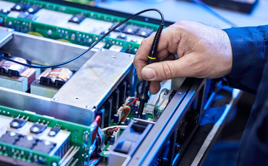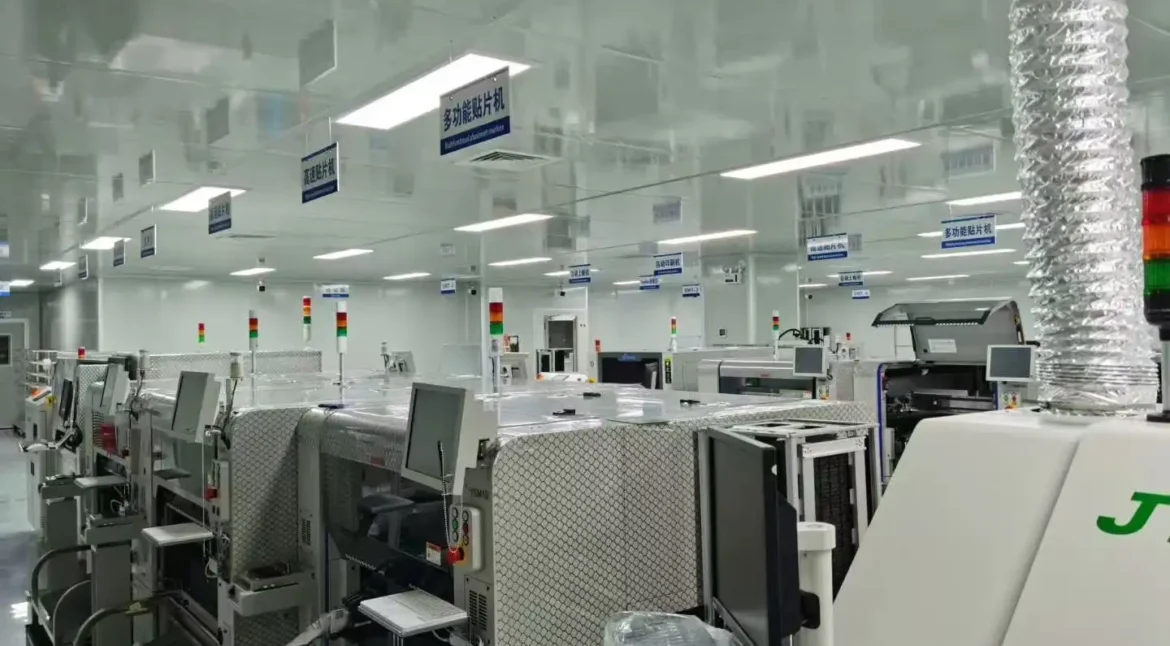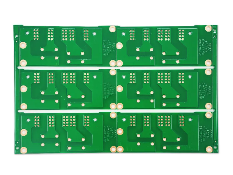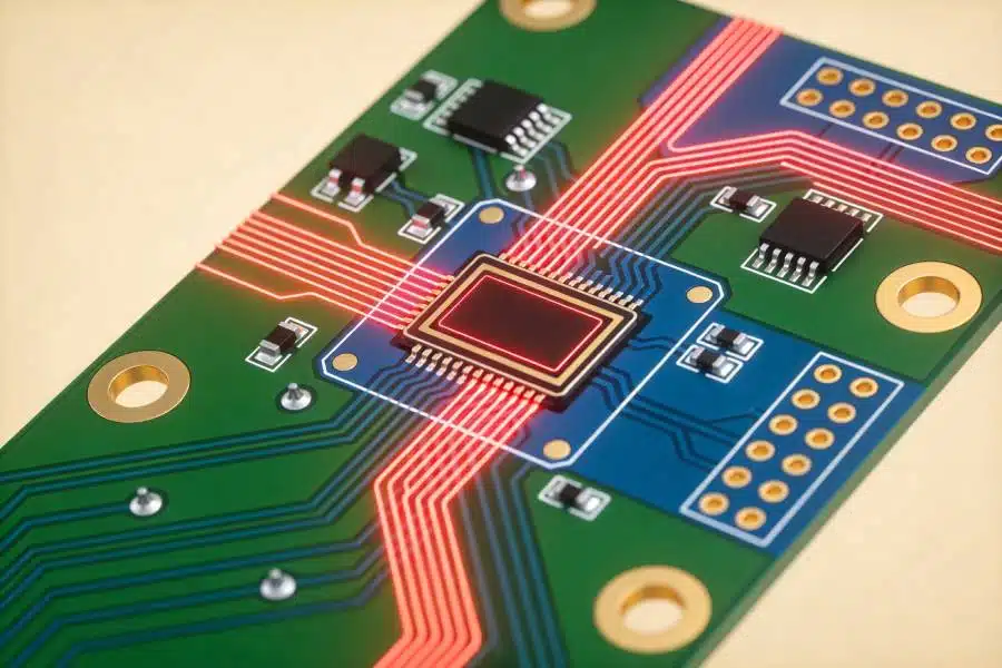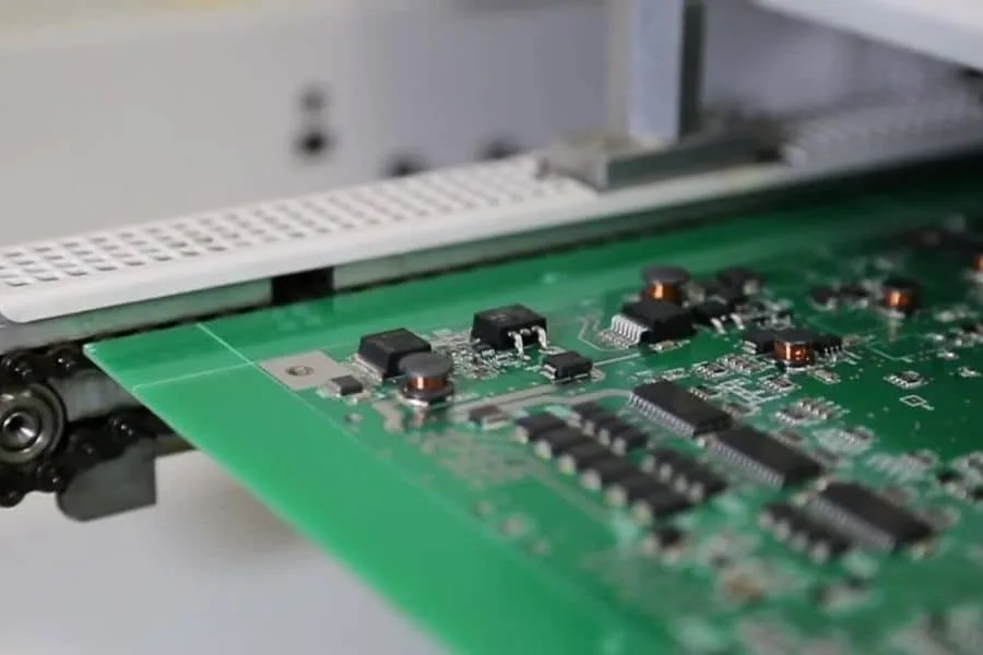
PCB Staking of Components: From Design to Repeatable Production Modern electronics depend on boards that are assembled correctly the first time. Every product – a phone, a charger, a medical instrument or an industrial controller – relies on thousands of solder joints that must conduct current for years. This article…
Environmental Controls in PCB Manufacturing: Waste Gas and Effluent PCB fabrication is a chemical process, and every chemical step produces a stream that has to be treated before it leaves the plant. The subject rarely appears in design reviews, but it does reach the designer in the form of material…
Ten-Layer Buried Via PCB: Process, Cost and Challenges Once a design passes eight layers, the outer layers fill up and the only remaining space is inside the board. A ten-layer buried via PCB solves that by moving the layer transitions inward, so that connections between inner layers never appear on…
Selective Plating Methods in PCB Fabrication Most plating is applied to a whole panel. Selective plating applies metal only where it is needed, which saves expensive material and avoids coating surfaces that must remain solderable. Four techniques are used in PCB work, and each suits a different geometry and production…
Conformal Coating Thickness: Standards and Measurement Conformal coating is a thin polymer film applied after assembly to keep moisture, dust, salt and chemical vapour away from the board surface. Its protection is a function of continuity rather than of thickness, but thickness is the parameter that can be specified, measured…
PCB Storage and Preservation: Shelf Life and Handling Rules Bare boards begin to change the moment they leave the production line. Copper oxidises, finishes age, absorbed moisture spreads through the laminate, and solderability falls. PCB storage is the set of practices that slow all of that down so that a…
PCB Quality Control: Inspection Stages and Standards Quality on a circuit board is built, not inspected. Inspection confirms that the process did what it was supposed to do, and a PCB quality control system that only looks at finished boards will find defects but never prevent them. The useful structure…
RFID PCB Design: Antenna, Frequency Band and Tag Assembly An RFID PCB carries an antenna and a tag or reader circuit on the same substrate. It is used where a label cannot survive, where the tag must be attached to a metal object, or where a reader has to be…
Plated Through Hole, Blind Via and Buried Via Compared A via looks like a hole and behaves like a very short piece of wire, but its real cost is space. Every via drilled through the whole board consumes a cylinder of routing area on every layer it passes through, and…
PCB Wire Routing Inside A Case: From Prototype to Volume Production Buyers and engineers often focus on the finished product and forget the production line behind it. In practice, most field failures can be traced back to process decisions made during assembly. Understanding PCB wire routing inside a case gives…