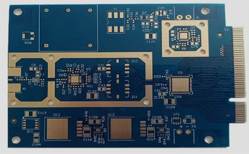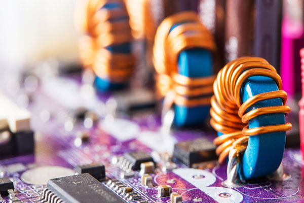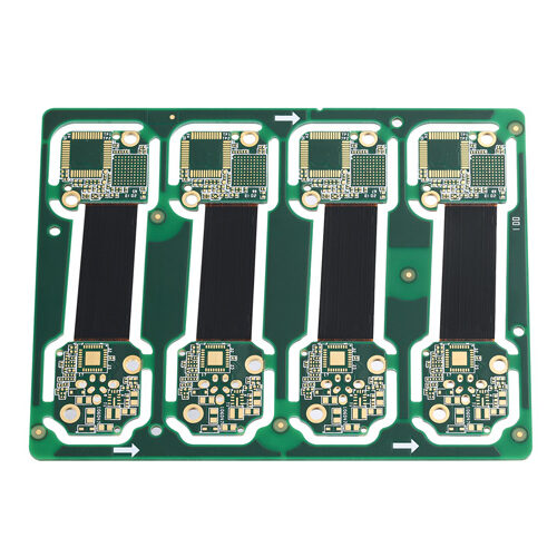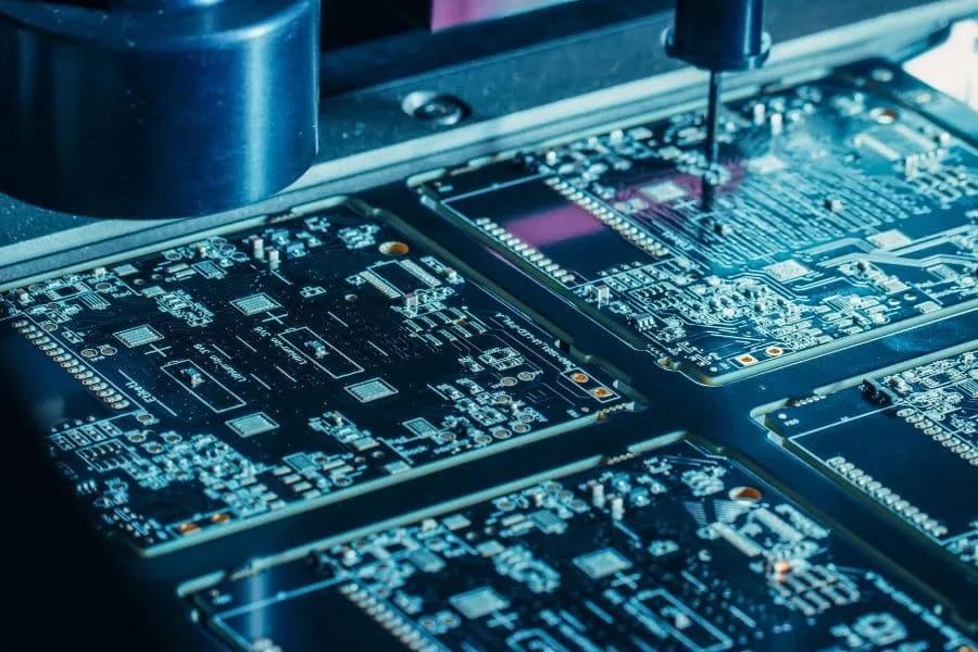

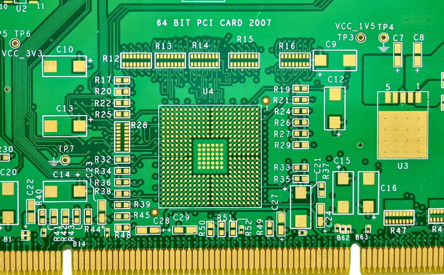
Smart Grid IoT PCB Cost: Structure, Bands and Design Choices Why Two Smart Grid Boards Can Differ in Price by a Factor of Five Utility companies, energy equipment manufacturers and IoT product teams all ask the same question about the hardware inside a smart meter, a distribution automation node, an…
PCB Stencil Nickel Plating: Coating the Stencil Walls Modern electronics depend on boards that are assembled correctly the first time. Every product – a phone, a charger, a medical instrument or an industrial controller – relies on thousands of solder joints that must conduct current for years. This article explains…
Microvia PCB Technology: Structures, Laser Drilling and Cost The Smallest Hole on the Board Does the Most Work As products have shrunk and their silicon has become denser, the conventional through-hole has become a bottleneck. It occupies routing area on every layer it passes through, it adds stub inductance that…
PCB Kapton Tape Masking: What Buyers and Engineers Should Check Modern electronics depend on boards that are assembled correctly the first time. Every product – a phone, a charger, a medical instrument or an industrial controller – relies on thousands of solder joints that must conduct current for years. This…
PCB Masking Tape for Gold Fingers: A Practical Manufacturing Guide Buyers and engineers often focus on the finished product and forget the production line behind it. In practice, most field failures can be traced back to process decisions made during assembly. Understanding PCB masking tape for gold fingers gives you…
IPC Class 3 PCB: Specifications, Process and Compliance The Acceptance Standard for Zero Defect Applications In aerospace avionics, medical devices, defence systems, power generation and high performance automotive powertrains, a PCB failure is not a warranty event. It is a safety incident, a mission loss or a regulatory problem. IPC…
Twenty Layer PCB Stackup: Design Rules and When You Need One When Eight or Twelve Layers Are Not Enough Most electronic systems are well served by eight, ten or twelve layer boards. As signal rates rise, integration density increases and systems accumulate more interfaces, the traditional multilayer stack reaches a…
PCB Legend Ink Jet Printing: Writing on the Board Electronics manufacturing has become a discipline of small details. Solder paste volumes, placement accuracy, temperature profiles and inspection limits all add up to the final result. This guide looks at PCB legend ink jet printing from the perspective of a PCBA…
Nelco PCB Materials: Properties, Selection and Performance When Standard FR-4 Runs Out of Headroom For most products, standard FR-4 is the right answer. It is cheap, well understood and easy to process. Push into high speed serial links, dense backplanes, 5G infrastructure, server platforms, aerospace systems or precision industrial control,…
PCB Scale Factor Compensation: Building In the Shrinkage Modern electronics depend on boards that are assembled correctly the first time. Every product – a phone, a charger, a medical instrument or an industrial controller – relies on thousands of solder joints that must conduct current for years. This article explains…