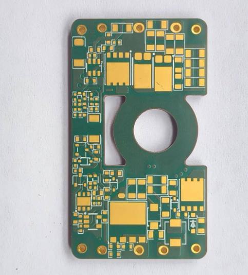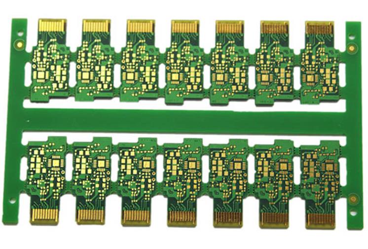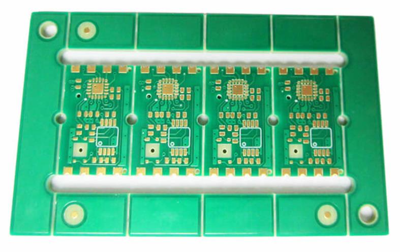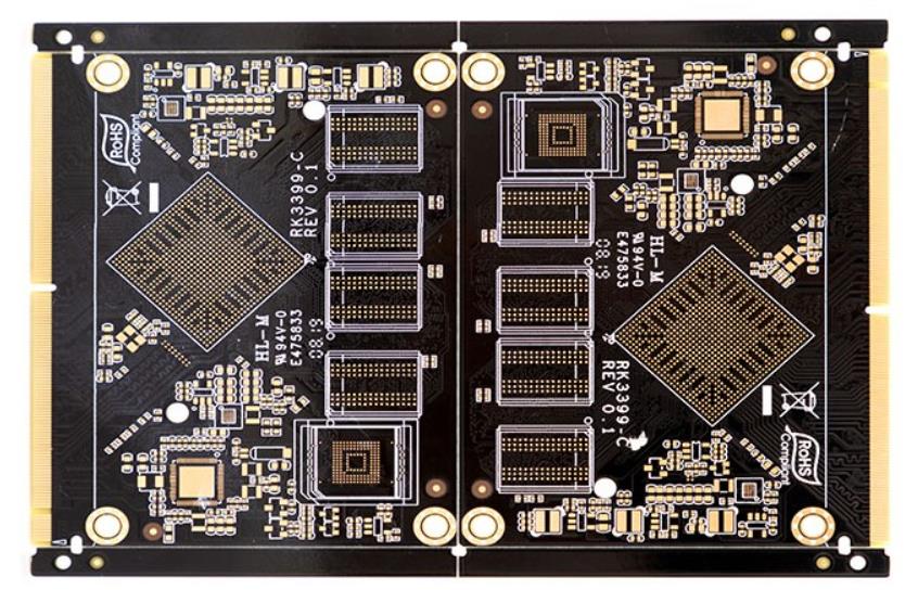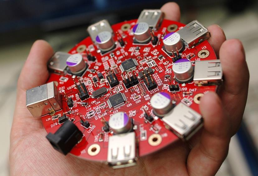
High Voltage PCB Material Selection Guide for Reliable Design Why High Voltage PCB Material Choice Matters Choosing a high voltage PCB material is the first and most important step in any power electronics design, because the laminate must do far more than carry current and signals. Ordinary products operate below…
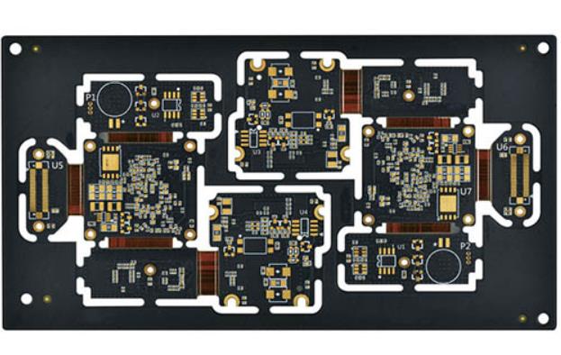
PCB Hole Wall Copper Defects and SAP Process Guide PCB hole wall copper defects such as copper particles and copper wires can appear during the fabrication of plated through-holes. These defects create rough hole walls, poor plating, opens, and reliability problems in the final PCBA. They are often caused by…
PCBA Processing Principles and DFM Checklist PCBA processing principles help engineers create boards that are easy to assemble, reliable in use, and low in manufacturing cost. A board designed without considering the assembly process may require extra processes, expensive fixtures, or unnecessary rework. Design for manufacturability turns the process requirements…
Buried Via vs Microvia: PCB Interconnect Comparison Guide Why Via Selection Matters Buried via and microvia are the two interconnect technologies that let a PCB fit more routing and better signal performance into a smaller board, and choosing between them is one of the first decisions that shapes the stack-up,…
PCBA Failure Analysis Techniques: Thermal Imaging Guide PCBA failure analysis techniques help engineers find faults quickly before a board is scrapped or a product fails in the field. A common approach uses infrared or thermal imaging to detect the heat produced by a defective component or short circuit. Because most…
SMT Stencil Production Process and Inspection Guide The SMT stencil production process starts with detailed requirements from the PCB assembly engineer and ends with a quality inspection before the stencil is shipped to the factory. A stencil controls the volume, position, and shape of solder paste deposited on every pad.…
Buried Via vs Microvia: PCB Interconnect Comparison Guide and polyimide pcb Why Via Selection Matters Buried via and microvia are the two interconnect technologies that let a PCB fit more routing and better signal performance into a smaller board, and choosing between them is one of the first decisions that…
Reflow Soldering Safety Precautions and Emergency Guide Reflow soldering safety precautions protect both operators and circuit boards during the most critical step of SMT production. The reflow oven operates at high temperature, moves boards along a conveyor, and can create dangerous conditions if the equipment is not monitored correctly. An…
AOI in PCB Detection: A Practical Review for Manufacturing Teams AOI in PCB detection is used to check the quality of solder paste printing, component placement, and soldering joints during SMT production. AOI stands for automatic optical inspection. The system captures images with CCD cameras, processes them with computer software,…
Solder Mask Dam: Design Rules, Width and Reliability Guide What a Solder Mask Dam Is A solder mask dam is the strip of solder mask material that separates two openings on a PCB, and it is the feature that stops solder from bridging between adjacent pads, pins or features. Where…