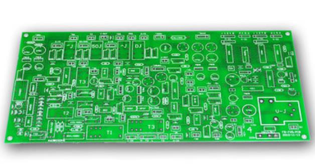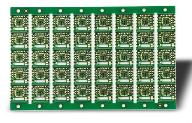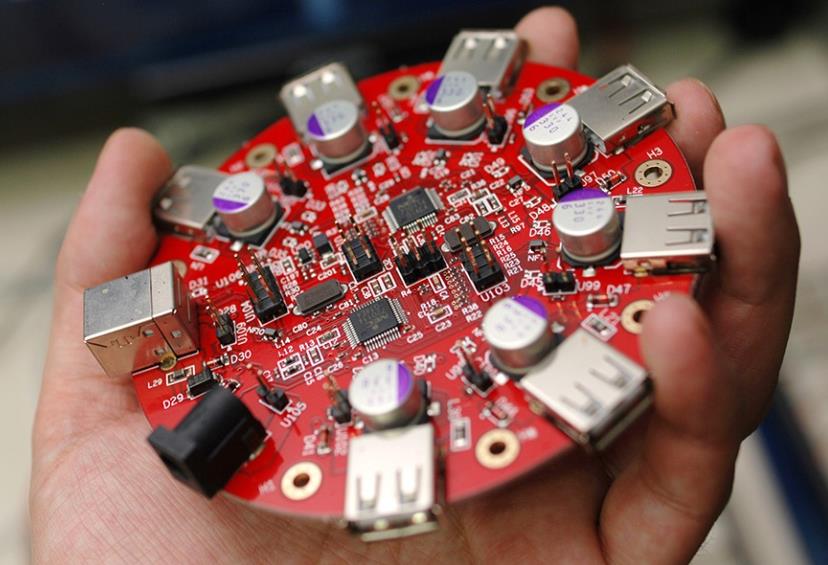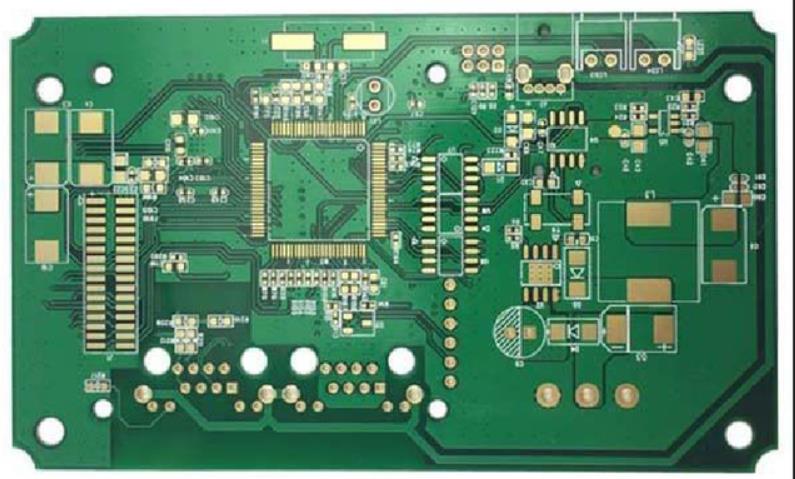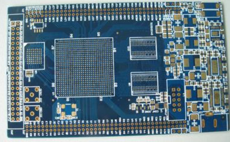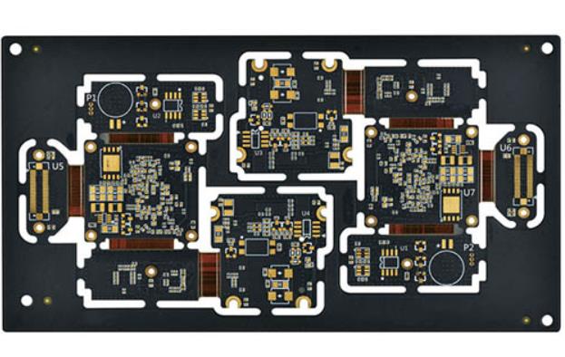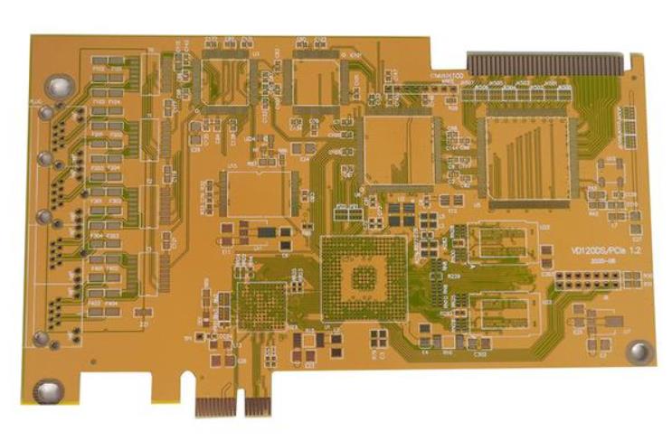
Solder Mask Misregistration: Causes, Effects and Prevention What Solder Mask Misregistration Is Solder mask misregistration is a manufacturing defect in which the solder mask layer does not align correctly with the copper pattern underneath, and it is one of the most common quality findings on printed circuit boards. When the…
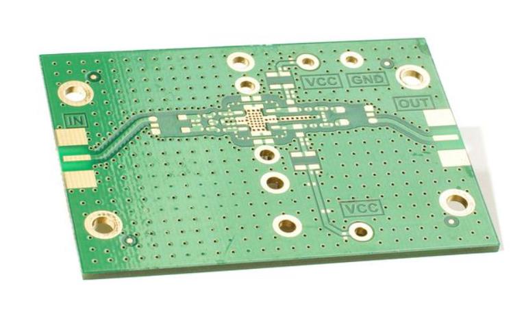
SMT Machine Online Programming and Changeover Guide SMT machine online programming lets an operator create or edit a placement program directly on the machine. The program defines the components, their coordinates, rotation angles, feeders, nozzles, and placement order. Online programming is commonly used when offline software is not available, when…
PCB Electroless Copper vs Electrolytic Copper Plating Guide Two Copper Plating Processes Electroless copper and electrolytic copper are the two plating processes that turn a bare drilled board into a board with conductive, plated holes, and understanding the difference matters for PCB quality, cost and reliability. Electroless copper deposits metal…
PCB Exposed Copper on Pads: Causes, Risks and Solutions PCB Exposed Copper: A Common Quality Issue Pcb exposed copper appears when copper that should be covered by solder mask or a protective finish becomes visible on the board surface, and it is one of the most frequent findings in PCB…
SMT Placement Machine Operation Process and Setup: Practical Process Controls The SMT placement machine operation process begins long before the first component is picked. The machine must be set up with the correct PCB, feeders, nozzles, and program data so that every component can be placed accurately without damaging the…
ENEPIG PCB Cost Guide: 2026 Price Factors Explained ENEPIG PCB Cost in 2026 The per-board cost of an enepig pcb, electroless nickel electroless palladium immersion gold, is never fixed. Board size, layer count, copper weight, line accuracy, hole structure, plating thickness, quantity, base material and test requirements all shape the…
X-ray Inspection of PCBA Boards: Complete Guide X-ray inspection of PCBA boards is used to see solder joints and internal structures that cannot be checked by eye or by an ordinary optical system. X-rays have a very short wavelength and very high energy, which allows them to pass through materials…
PCB Trace Antenna vs Chip Antenna: Cost and RF Guide PCB Trace Antenna vs Chip Antenna Antenna selection shapes wireless performance, product size and cost for Bluetooth, Wi-Fi, IoT, GPS, Zigbee and other radio products, and the two most common approaches are the pcb trace antenna and the chip antenna.…
SMT Placement Head Guide: A Practical Manufacturing Guide An SMT placement head is the intelligent robotic arm at the center of a pick-and-place machine. It moves in three dimensions, picks components from feeders, corrects their orientation, and places them on the PCB at the exact pad position. The placement head…
Any Layer HDI PCB Cost Guide: 2026 Manufacturing Factors Any-Layer HDI PCB Cost in 2026 Smart terminals, 5G communication gear, automotive electronics, medical devices and high-performance computing keep demanding smaller boards with more integrated function, and any layer hdi pcb technology answers that demand with laser microvias, sequential build-up, fine…