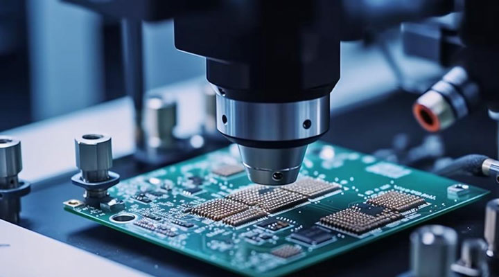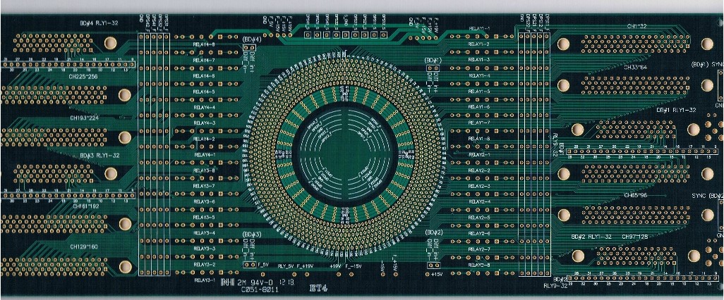
Laser Via Drilling: Energy Density and Taper Control Laser via drilling makes the small holes that connect the layers of a high density board. The beam removes dielectric by vaporising it, and the process stops on the copper of the target layer, which acts as a natural etch stop. That…

Hot Air Drying After Cleaning: Water Spots and Residue Cleaning a printed circuit assembly ends with drying, and the drying step decides what the cleaning leaves behind. Water that evaporates from a surface deposits whatever was dissolved in it as a ring of residue in the same place. If the…
Component Cracking in Reflow: Thermal Shock and Moisture A cracked component is a failure that is often invisible at the end of the assembly line and certain to appear in the field. The crack may run through a ceramic body, through the encapsulation of a plastic package or through the…
Hole Wall Voids: Causes and Plating Coverage Control A hole wall void is a break in the plated copper that covers the barrel of a drilled hole. The break may expose the laminate underneath or it may be a thin spot where the plating is discontinuous. Either way the barrel…
Through Hole Fill: Vertical Fill and Solder Volume Control Through hole fill is the proportion of a plated barrel that is occupied by solder after the joint has formed. Barrel fill, more formally called vertical fill, is expressed as a percentage of the board thickness, and it is specified separately…
PCB Annular Ring Specification: Practical Process Controls Buyers and engineers often focus on the finished product and forget the production line behind it. In practice, most field failures can be traced back to process decisions made during assembly. Understanding PCB annular ring specification gives you a practical advantage when you…
PCB Etch Factor Setup: From Design to Repeatable Production Electronics manufacturing has become a discipline of small details. Solder paste volumes, placement accuracy, temperature profiles and inspection limits all add up to the final result. This guide looks at PCB etch factor setup from the perspective of a PCBA factory…
PCB Etch Factor Defects: What Goes Wrong Modern electronics depend on boards that are assembled correctly the first time. Every product – a phone, a charger, a medical instrument or an industrial controller – relies on thousands of solder joints that must conduct current for years. This article explains PCB…
PCB Etch Factor Standards: Agreeing the Rules Buyers and engineers often focus on the finished product and forget the production line behind it. In practice, most field failures can be traced back to process decisions made during assembly. Understanding PCB etch factor standards gives you a practical advantage when you…
Presser Foot and Stack Clamping in PCB Drilling Every drilling machine presses the stack against the tool with a foot that surrounds the spindle. The presser foot flattens the entry material onto the panel, holds the layers in register and limits the vibration that the drill induces. Stack clamping is…