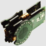
PCB Back Drilling Limits: Where the Edges Are
Back drilling removes the unused copper barrel that extends below the target layer in a plated through hole. The stub that remains after drilling acts as a small antenna at high frequency. At low speeds it does nothing, but at multi-gigabit rates it reflects energy and closes the eye diagram. The limits of the process sit where the remaining stub, the drill depth tolerance and the panel thickness stop working together. This review sets out those edges from the shop floor upward.
The technique is common on thick backplanes, high-layer-count server boards and any design that carries fast differential pairs through long vias. It is not a universal step, and it adds cost to every hole it touches. Engineers should decide which vias need the treatment and which can stay untouched. Buyers should understand what the extra step does to yield, lead time and price before they approve it. The sections below explain the decisions and the checks that keep the result predictable.
What Back Drilling Removes
A plated through hole is drilled through the full stack and plated, so copper lines the entire barrel. Signal layers near the top use only part of that barrel, and the rest hangs below as a stub. At low frequency the stub is invisible. At high frequency it behaves like a short transmission line and creates a resonance that distorts the signal. Back drilling re-enters the hole from the opposite side and cuts away the unused copper, leaving a shorter stub above the target layer.
The process uses a drill bit slightly larger than the original hole so it clears the plating without touching the walls that carry the signal. Depth control is the whole game. Cut too little and a stub remains. Cut too deep and the bit damages the barrel at the target layer or nicks an adjacent trace. The window between those two failures is the practical limit of the process, and it narrows as boards get thicker and layers get denser.
Depth Tolerance Drivers
Depth accuracy depends on the drilling machine, the stackup and the panel itself. The machine references the surface, so any variation in board thickness shifts the cut. Lamination presses do not produce perfectly uniform thickness across a panel, and the difference between nominal and actual can exceed the tolerance the design allows. A board built to a loose thickness spec will fight the back drill every time.
Drill bit wear matters as well. A worn bit wanders and cuts a shallower or deeper hole than the program expects. Good shops track bit life and replace tools on a schedule rather than on failure. Z-axis control, spindle runout and the accuracy of the depth sensor all feed the same number. When a design pushes close to the edge, the fabricator should confirm the machine capability before quoting. The quality management system should hold those calibration records.
Design Rules That Help
The design sets the target layer, the allowed stub and the clearance around the hole. A generous anti-pad around the back-drilled via gives the larger bit room to cut without touching neighboring copper. Tight anti-pads force a smaller step-up in bit size, which leaves more stub and reduces the benefit. Designers should check this clearance before they commit to the technique on a dense board.
Layer assignment matters too. A signal that runs on a layer close to the surface needs a shallow cut, which is easier to hold. A signal buried near the middle of a thick board needs a deep cut, and the tolerance grows with depth. Spreading critical signals across layers with different depths complicates the drill program. Grouping fast traces on similar depths keeps the process simpler and the yield higher.

Stackup and Material Effects
Thicker boards make depth control harder because a small percentage error becomes a larger absolute error. High-layer-count backplanes sit at the difficult end of the range, and some designs simply cannot hold a tight stub without special equipment. The fabricator should state the achievable stub for the stackup rather than promise a number that suits a thin board. Buyers should ask for that figure in writing before layout is frozen.
Material choice also plays a part. Resin systems with different glass content and fill behave differently under the drill, and some are more prone to smear or chipping at the exit. The drill parameters are tuned to the material, so a stackup change late in the project can reopen the depth question. Keep the stackup stable once the back drill is qualified.
Drilling and Inspection Risk
The back drill is a second operation on a finished hole, so it carries risk that the first drill does not. Chipping at the cut edge, copper smearing and barrel damage are the common failure modes. A bit that is slightly off center can graze the plating on the signal side. These defects are hard to see from the surface, which makes inspection important and makes sampling alone unreliable.
Cross sectioning is the clearest check because it shows the remaining stub directly. Shops often cut a coupon from the panel edge and measure the stub under magnification. X-ray and optical methods help on production panels, but the cross section remains the reference. The fabricator should record the measured stub against the target and keep the data with the lot. That record is what proves the process held on the day.
Electrical Test Coverage
Back drilling can open a barrel or weaken a connection, so electrical test must confirm continuity after the cut. A net that passes before back drilling and fails after it points straight at the operation. Test coverage should include the vias that were cut, not just the ones that were left alone. A structured PCBA testing plan covers this at the bare board stage and again after assembly.
High-speed verification is a separate question. A time domain reflectometry measurement can show the stub effect on a test coupon, and it gives the design team real data instead of a promise. Not every order needs it, but a first article on a new stackup benefits from the check. Buyers should agree on which measurements are reported and which are skipped, so expectations match the price.
Cost and Yield Tradeoffs
Every back-drilled hole adds a drilling step, a tool change and an inspection burden. The cost per hole is small, but a board with thousands of vias multiplies it quickly. Designers should cut only the vias that carry fast signals and leave the rest alone. That decision alone can change the price of a large backplane by a wide margin, and it costs nothing at the layout stage.
Yield also moves. A tight stub target raises the scrap rate because more panels fall outside the window. A looser target that still meets the signal requirement is often the better commercial choice. The right answer comes from the electrical need, not from a habit of cutting as deep as possible. Engineers and buyers should agree on the stub target together and write it into the fabrication note.
Working With the Fabricator
The fabrication note should state the target layer, the allowed stub, the anti-pad clearance and the vias in scope. Ambiguity here is expensive, because the shop will build to its own assumption. A short table in the drawing removes the guesswork and gives both sides a reference when a question arises. The rapid PCBA prototyping stage is the right time to test that note on a real panel.
Ask the fabricator for the achievable stub on your stackup, the inspection method and the records you will receive. A shop that answers with measured data and a clear method is easier to trust than one that quotes a number without context. For volume programs, confirm how the process is monitored across lots and who reviews the trend. The same discipline that supports high-volume PCB assembly applies here, because a stable back drill is a process control problem before it is a drilling problem.
Prototypes teach the most. A small pilot batch reveals depth behavior, chip risk and test results before thousands of panels are committed. Treat the pilot as part of the qualification rather than an extra cost. When the design moves to SMT PCB assembly, the bare board records should travel with the lot so the assembly team knows which vias were cut. That continuity keeps the whole build traceable from drill to ship.
The edge of the process is not a single number. It is the point where stub target, stackup thickness, machine capability and inspection method stop agreeing. Push past it and the failures appear as intermittent signal problems that are hard to trace. Stay inside it with a written target and measured records, and the technique does its job quietly. Buyers should confirm the stub figure and the inspection method before release, and engineers should design the clearance that makes the cut possible.