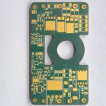
PCB Classification: Three Main Types Explained
PCB classification starts with one simple question: how many copper layers carry the circuit? The answer shapes cost, routing freedom, and the process steps a factory must control. Most buyers meet this choice early, when a design moves from a breadboard idea into a real board. The three main types below cover nearly every product, from a toy to a server. Knowing where a design sits helps you plan both budget and supplier.
The layer count is not just a number on a drawing. It changes drilling, lamination, plating, and inspection demands at every stage. A single-sided board and an eight-layer board may share the same outline, yet their process routes differ sharply. Buyers who understand that difference ask better questions and read quotations more carefully. Engineers who understand it choose a stackup that fits the product instead of guessing.
Single-Sided Boards
A single-sided board carries copper traces and pads on one face only. The other face is bare insulating substrate, often with nothing more than silkscreen. Routing must finish on that one side, so traces cannot cross each other through vias. Designers therefore work around crossings with careful placement and short links. This limit keeps the board cheap, because drilling and plating steps drop away.
Fabrication is short and predictable. The factory etches one copper layer, then adds solder mask and legend. There is no lamination cycle and no plated through hole to control. That simplicity suits high volumes of low-complexity circuits, where the unit price matters more than routing density. It also makes the board easy to inspect, since every trace is visible from one side.
Typical uses include toys, simple chargers, indicator panels, and basic remote controls. These products need few connections and tolerate a plain layout. The tradeoff is clear: any design change that needs a crossing forces a jump to two layers. Buyers should confirm the design really fits one side before committing to tooling. A late switch to double-sided adds cost and delay.
Double-Sided Boards
A double-sided board puts copper on both faces and joins the layers with plated vias. Routing space roughly doubles, so crossings become manageable and layouts stay compact. This is the workhorse of general electronics and the type most projects use. Microcontroller boards, smart home modules, and small control circuits all fit here. The balance of cost and capability is hard to beat.
Adding the second layer brings new process steps. The factory must drill, plate the barrel, and image both sides with proper registration. Vias need clean walls and reliable plating, or an intermittent connection appears later. Buyers should ask how the supplier controls drill registration and plating thickness. These checks separate a stable double-sided build from a risky one.
Design rules matter more here than on a single-sided board. Keep power and ground traces wide, and keep signal paths short and direct. Place connectors near the board edge and group related functions together. Good layout reduces the need for extra layers later. For layout support, our team handles PCB design and layout from schematic through routing.
Multilayer Boards
A multilayer board stacks three or more copper layers and presses them into one solid unit. Common builds are four, six, and eight layers, with dense products going higher. Inner layers often serve as power and ground planes, while outer layers carry signals. That arrangement shortens return paths and improves signal integrity. It also supports fine traces and dense component placement.
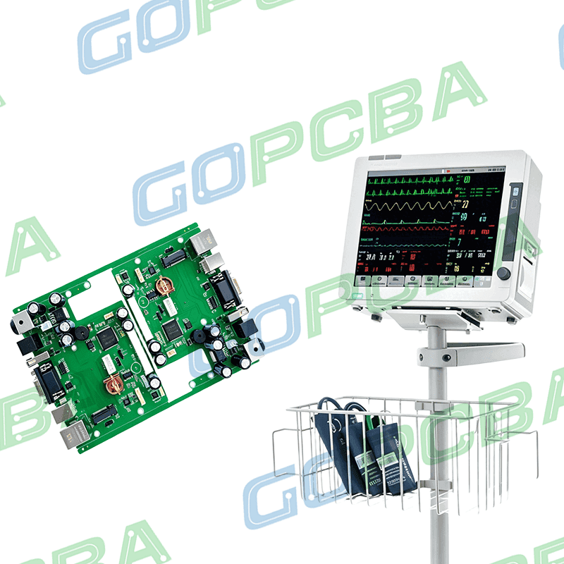
The process grows harder with every layer. Lamination must bond the stack without voids or resin starvation. Drill depth and registration must stay tight across the whole panel. Inner-layer features must align before pressing, because a misregistration cannot be fixed afterward. Each added layer raises the cost of scrap, so process control carries real money.
These boards suit high-speed, miniaturized, and precision equipment. Phone mainboards, computer boards, and industrial controllers rely on them. The cost is higher, so beginners rarely need them early. Engineers should justify each added layer with a real routing or noise problem. A stackup built on habit rather than need wastes budget.
Stackup Choices
The stackup defines layer order, dielectric thickness, and copper weight. It decides impedance, crosstalk, and how easily the board can be fabricated. A four-layer board with solid ground and power planes often outperforms a poorly planned six-layer build. Engineers should place planes next to signal layers to keep return currents short. The stackup should be agreed with the factory before routing starts.
Copper weight affects current capacity and etch control. Heavier copper handles more current but etches less finely. Dielectric thickness affects impedance and must match the design targets. Buyers should ask for the proposed stackup in writing and check it against the design rules. A stackup that the factory cannot build reliably will cause problems at the first article.
Lamination Control
Lamination bonds the layers under heat and pressure, and it decides whether the board stays flat and void free. Resin must fill the gaps between copper features without starving the bond. Trapped air or moisture can cause blisters during assembly reflow. Factories control this with proper bake cycles, press profiles, and material storage. Buyers should ask how panels are dried before pressing.
Material choice matters as much as the press. Resin content, glass style, and copper treatment all affect the bond. A supplier that changes laminate without notice can shift the process quietly. Qualified materials and approved alternates reduce that risk. Documentation of the laminate lot helps trace any later field issue.
Drilling Risk
Drilling is where many multilayer problems begin. A hole must pass through the correct layers and land on the target pad. Drill wander, poor registration, or worn bits can miss the pad or damage the barrel. Plating then has to coat the wall evenly to form a reliable connection. Small holes and thick boards make this harder.
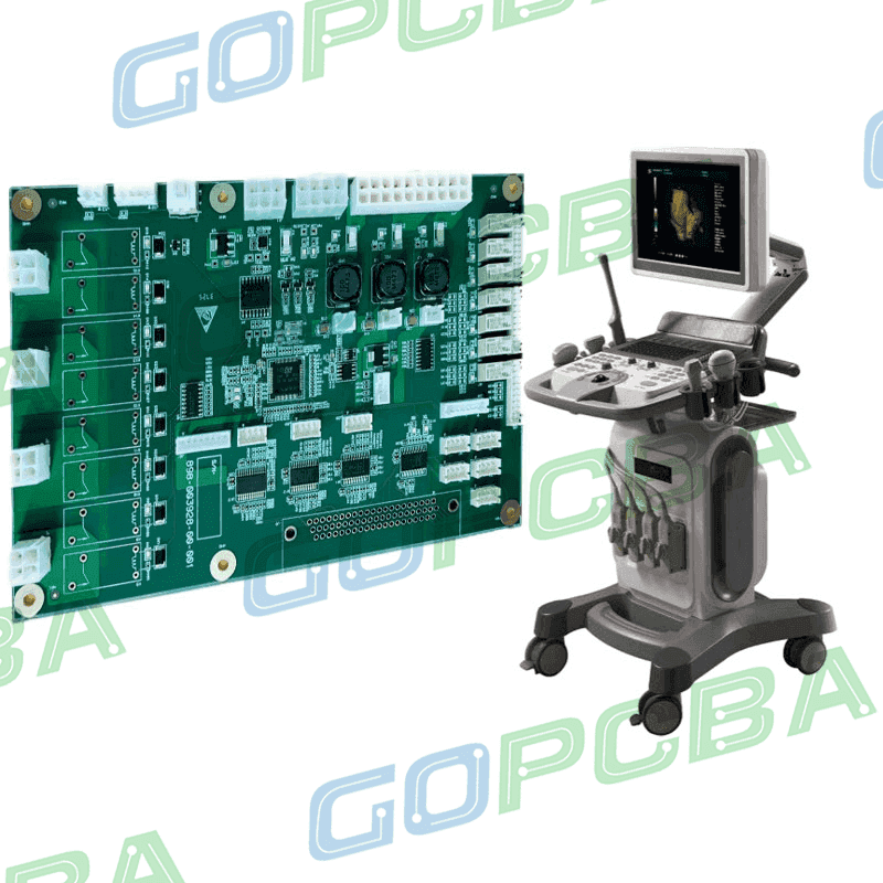
Vias also affect routing and cost. Each drill hit adds time, and dense via counts raise the price. Designers should use the largest via that fits the routing need. Buyers should confirm the factory controls drill registration and inspects hole walls. A cracked barrel may pass a quick check and fail in the field.
Test Coverage
Test proves the board matches the design before assembly begins. Electrical test checks for opens and shorts across the netlist. Visual inspection catches mask, legend, and surface defects. For assembled boards, in-circuit and functional test add another layer of confidence. Our PCBA testing service covers these steps in one flow.
Test coverage should match the risk of the product. A simple single-sided board needs less than a dense multilayer design. Buyers should ask which tests run, what passes, and what records come with the shipment. A test report is worth more than a verbal promise. It shows the board was checked against a defined plan.
Choosing the Right Type
Start with the circuit, not the price list. Count the nets that must cross and check whether one side can carry them. If crossings appear, two layers usually solve the problem at modest cost. Move to multilayer only when routing density, impedance, or noise control demands it. Each step up adds process steps and cost.
Volume and reliability also shape the choice. A high-volume simple product favors the cheapest board that works. A product with tight signal requirements favors a planned stackup and solid planes. Buyers should compare suppliers on process control, not only unit price. A cheap board that fails in the field costs far more than a well-built one.
When the design is ready, the next step is assembly. Our SMT PCB assembly lines handle surface-mount builds with paste inspection and optical checks. For mixed technology, PCB assembly covers through-hole and odd-form parts. Buyers planning a full program can use turnkey PCB assembly to combine fabrication, sourcing, and build under one schedule.
The final takeaway is simple. Choose the lowest layer count that meets the routing and signal needs, then confirm the factory can control that process. Ask for the stackup, drill and plating controls, and the test plan in writing. Those documents tell you whether the board will be repeatable, not just buildable once.