Estimating the cost of a printed circuit board project is an essential part of electronics product development. Engineers and purchasing teams need to balance electrical performance, manufacturing quality, production volume, delivery requirements, and budget constraints before moving a design into production.
A PCB cost calculator provides a convenient way to estimate the fabrication cost of a PCB based on key design and production parameters. However, the fabrication quote represents only one part of the total project budget. A complete PCB project may also include PCB assembly, electronic components, testing, tooling, engineering services, packaging, and shipping.
Whether you are developing a PCB prototype, preparing for small-batch production, or planning volume manufacturing, understanding these cost drivers can help you make better engineering and purchasing decisions.
This guide explains how a PCB cost calculator works, which factors affect PCB manufacturing cost, how to estimate the total project budget, and how design optimization can reduce unnecessary expenses.
What Is a PCB Cost Calculator?
A PCB cost calculator is a quotation or estimation tool that calculates an approximate PCB manufacturing price based on the technical specifications and order requirements provided by the customer.
Depending on the manufacturer, a calculator may allow users to enter parameters such as:
- Board dimensions
- PCB layer count
- PCB material
- Copper thickness
- Surface finish
- Minimum trace width and spacing
- Minimum hole diameter
- Via structure
- PCB quantity
- Production technology
- Special manufacturing requirements
For example, a simple two-layer FR-4 PCB with standard dimensions and a large production quantity will normally have a lower unit cost than a small-volume, high-layer-count PCB manufactured with advanced materials and fine-line HDI technology.
A cost calculator is useful because it allows engineers to evaluate different design configurations before committing to production.
However, it should be treated as an initial cost estimation tool, not necessarily as the final commercial quotation. The final price may change after engineering review, DFM analysis, material confirmation, and manufacturing assessment.
What Information Does a PCB Cost Calculator Need?
The accuracy of a PCB cost calculator depends largely on the quality of the input information.
1. PCB Board Size
Board dimensions directly influence material consumption and panel utilization.
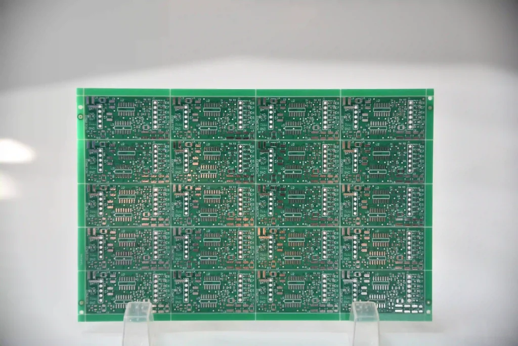
For example, a smaller PCB may allow a manufacturer to place more individual boards onto a standard production panel, improving material utilization and reducing the effective cost per unit.
When optimizing board size, engineers should consider both electrical requirements and panelization efficiency.
Reducing board dimensions can lower material consumption, but excessive miniaturization may increase routing complexity and manufacturing difficulty.
2. Number of PCB Layers
The PCB layer count is one of the most important cost factors.
Typical configurations include:
- Single-layer PCB
- 2-layer PCB
- 4-layer PCB
- 6-layer PCB
- 8-layer PCB
- 10-layer and higher multilayer PCB
More layers generally require additional laminate, copper, lamination cycles, drilling, plating, and inspection processes.
However, reducing layer count solely to save money is not always appropriate. The correct layer count must satisfy:
- Routing requirements
- Signal integrity
- Power distribution
- Thermal management
- Controlled impedance
- EMC/EMI requirements
- Component density
The goal should be cost-effective engineering, rather than simply minimizing the number of layers.
3. PCB Material
Material selection has a major impact on PCB manufacturing cost.
Common materials include:
- Standard FR-4
- High-Tg FR-4
- Halogen-free materials
- Low-loss laminates
- High-frequency materials
- PTFE-based materials
- Polyimide
- Aluminum and other metal-core materials
For general-purpose electronics, standard FR-4 may provide an effective balance between performance and cost.
For high-speed or RF applications, however, engineers may need specialized materials with controlled dielectric properties and low signal loss.
Therefore, material selection should be based on actual electrical, thermal, and mechanical requirements rather than price alone.
4. Copper Thickness
Standard PCB copper thickness is often specified around 1 oz, but applications requiring higher current capacity may require thicker copper.
Higher copper weight can increase manufacturing cost because it may require additional plating and etching considerations.
Thicker copper is commonly used in:
- Power electronics
- Battery management systems
- Automotive power systems
- Industrial equipment
- High-current circuits
The copper thickness should therefore be optimized according to current-carrying requirements and thermal performance.
5. Surface Finish
The selected PCB surface finish also affects cost.
Common options include:
- HASL
- Lead-free HASL
- ENIG
- ENEPIG
- OSP
- Immersion tin
- Immersion silver
HASL is generally suitable for many conventional applications and can provide a cost-effective solution.
ENIG may be preferred for fine-pitch components, high-density boards, and applications requiring a flatter surface.
The most economical finish is not always the best technical choice. Surface finish should be selected according to component package requirements, solderability, storage conditions, reliability, and application environment.
6. Trace Width and Spacing
Minimum trace width and spacing have a direct impact on manufacturing difficulty.
Standard designs are generally easier and less expensive to manufacture than boards requiring extremely fine traces and spaces.
Fine-line requirements may require:
- Advanced imaging
- Tighter registration control
- More precise etching
- Additional process controls
- Advanced inspection
Therefore, designers should avoid unnecessarily aggressive trace and spacing requirements when conventional dimensions can satisfy the electrical requirements.
7. Drilling and Via Requirements
The number, size, and type of holes can influence the PCB fabrication cost.
Common structures include:
- Through-hole vias
- Blind vias
- Buried vias
- Microvias
- Via-in-pad
A conventional through-hole via is generally simpler to manufacture than a laser-drilled microvia.
For HDI PCB designs, microvias and sequential lamination can significantly increase manufacturing complexity.
Designers should therefore use advanced via structures only when required by routing density, component pitch, or electrical performance.
Connecting PCB Cost Per Unit to the Total Project Budget
The PCB cost per unit is an important starting point, but it does not represent the complete cost of an electronics project.
A more useful calculation is:
Total PCB Project Cost = PCB Fabrication + PCB Assembly + Components + Testing + Tooling/Engineering + Packaging + Shipping
This broader approach helps prevent unexpected expenses during the development and production stages.
Main Components of a PCB Project Cost
1. PCB Fabrication Cost
The basic fabrication cost includes manufacturing the bare PCB.
It is affected by:
- PCB dimensions
- Layer count
- Material
- Copper thickness
- Surface finish
- Minimum trace and spacing
- Hole structure
- Quantity
- Special processes
For example, a 2-layer FR-4 board manufactured in a large quantity may have a significantly lower unit cost than a small batch of 10-layer HDI boards.
2. PCB Assembly Cost
If the project requires PCB assembly, assembly costs must be added to the fabrication cost.
Major assembly cost drivers include:
- Number of components
- Component package types
- SMT component density
- Through-hole components
- Number of assembly sides
- Stencil requirements
- SMT setup
- Soldering process
- Inspection requirements
- Testing requirements
For example, a board containing hundreds of small components generally requires more placement and inspection resources than a simple board with a small component count.
3. Component Cost
For a complete PCBA project, the electronic components may represent a substantial portion of the total project budget.
The BOM may include:
- Resistors
- Capacitors
- Diodes
- Transistors
- Connectors
- ICs
- Sensors
- Modules
- Power devices
Component prices can fluctuate because of availability, manufacturer, lifecycle status, purchasing quantity, and market conditions.
Therefore, component sourcing should be considered together with PCB fabrication and assembly.
4. Testing Cost
Testing requirements depend on the product and application.
Possible testing methods include:
- Electrical testing
- Flying probe testing
- ICT
- Functional testing
- AOI
- X-ray inspection
- Burn-in testing
- Reliability testing
A simple prototype may require only visual and electrical inspection, while automotive, medical, aerospace, or industrial electronics may require more comprehensive verification.
5. Tooling and Engineering Cost
Some PCB projects require additional engineering or tooling costs.
These may include:
- Stencil
- Special fixtures
- Test fixtures
- Engineering setup
- Special drilling
- Special lamination
- Custom packaging
For prototypes, these fixed costs can have a greater impact on the effective unit price because they are distributed across a smaller number of boards.
6. Packaging and Shipping
The final project cost should also include packaging and logistics.
Shipping costs depend on:
- Shipment weight
- Package dimensions
- Destination
- Shipping method
- Delivery speed
- Customs requirements
For international projects, transportation should be considered when comparing PCB suppliers from different regions.
How to Use a PCB Cost Calculator
A practical PCB cost estimation process can be divided into several steps.
Step 1: Prepare Your PCB Specifications
Prepare the basic manufacturing information:
- Board size
- Layer count
- Material
- Copper thickness
- Surface finish
- Quantity
- Minimum trace/spacing
- Hole requirements
For PCBA projects, also prepare:
- BOM
- Gerber files
- Pick-and-place files
- Assembly drawings
- Component specifications
Step 2: Enter the Core Parameters
Enter the PCB dimensions, layer count, material, quantity, and other required specifications into the calculator.
The tool will generate an initial fabrication estimate.
Step 3: Compare Different Configurations
Test alternative configurations to understand their cost impact.
For example:
Option A: 4-layer standard FR-4 PCB
Option B: 6-layer standard FR-4 PCB
Option C: 4-layer high-Tg PCB
Comparing the options can help engineers determine whether a more expensive specification is technically necessary.
Step 4: Perform DFM Analysis
After obtaining an initial estimate, conduct a DFM analysis.
DFM can identify:
- Excessively small holes
- Tight trace spacing
- Insufficient clearances
- Unnecessary tolerances
- Difficult component footprints
- Manufacturing risks
- Inefficient panelization
Correcting these issues before production can reduce both cost and manufacturing risk.
Step 5: Add Assembly and Component Costs
For a complete PCBA project, combine the PCB fabrication estimate with:
- Component cost
- SMT assembly
- THT assembly
- Stencil
- Inspection
- Functional testing
- Packaging
- Shipping
This produces a much more realistic project budget.
PCB Cost Calculation Example
Consider a hypothetical project with the following specifications:
- PCB size: 100 mm × 100 mm
- Layers: 4
- Material: FR-4
- Copper: 1 oz
- Surface finish: Lead-free HASL
- Quantity: 100 pcs
- Components: 50 per board
- Testing: Basic functional testing
A simplified project budget could be structured as follows:
| Cost Category | Example Cost |
|---|---|
| PCB fabrication | $500 |
| PCB assembly | $350 |
| Components | $1,000 |
| Testing | $200 |
| Shipping | $50 |
| Estimated total | $2,100 |
This example is for cost estimation only. Actual PCB and PCBA pricing varies according to design complexity, materials, quantity, component availability, testing requirements, production location, and supplier capabilities.
The most important lesson is that PCB cost per unit is only one part of the total project cost.
How to Reduce PCB Manufacturing Cost
Cost reduction should begin during PCB design rather than after production.
1. Optimize Board Size
Reducing unnecessary board area can improve material utilization and panel efficiency.
However, the board should not be made smaller if doing so creates routing, thermal, assembly, or reliability problems.
2. Avoid Unnecessary Layer Count
Use the minimum practical number of layers that satisfies electrical and mechanical requirements.
Reducing a 6-layer design to 4 layers can reduce cost when routing and signal integrity requirements allow it.
3. Use Standard Materials When Possible
Standard FR-4 is generally more economical than specialized high-frequency or low-loss laminates.
However, specialized materials should be used when required by:
- High-speed signals
- RF performance
- Thermal requirements
- High-frequency applications
- High-reliability environments
4. Use Standard Manufacturing Rules
Avoid unnecessarily tight:
- Trace widths
- Trace spacing
- Hole sizes
- Annular rings
- Board tolerances
A PCB designed around the manufacturer’s standard process window is usually easier and more economical to produce.
5. Optimize Panelization
Effective panelization can improve material utilization and reduce waste.
A professional PCB manufacturer can evaluate how the board should be arranged on a manufacturing panel before production.
6. Increase Production Quantity When Appropriate
Economies of scale can significantly affect PCB cost per unit.
Fixed costs such as engineering setup, tooling, and testing can be distributed across more boards as production volume increases.
However, customers should avoid ordering excessive quantities simply to obtain a lower unit price. Inventory cost, product lifecycle, and component obsolescence should also be considered.
Lead Time and PCB Cost
Lead time is another important part of the total manufacturing cost.
Urgent production may require:
- Priority scheduling
- Expedited material procurement
- Quick-turn engineering
- Additional production resources
- Expedited shipping
As a result, quick-turn PCB manufacturing may cost more than standard production.
For projects with flexible schedules, allowing sufficient manufacturing time can reduce the premium associated with expedited production.
The best strategy is to balance PCB cost, lead time, and inventory requirements.
Does Manufacturing Location Affect PCB Cost?
Yes. Manufacturing location can affect:
- Labor cost
- Material sourcing
- Factory overhead
- Logistics
- Import duties
- Supply-chain efficiency
- Production scale
However, the lowest quoted manufacturing price does not necessarily produce the lowest total cost.
A more useful comparison is total landed cost, which includes:
PCB Price + Assembly + Components + Testing + Shipping + Duties + Engineering + Inventory Cost
This approach provides a more realistic comparison between suppliers.
How Kingda Helps Optimize PCB Project Costs
As an experienced PCB manufacturer and PCB assembly service provider, Kingda provides integrated manufacturing solutions designed to support customers from initial design validation through production.
Kingda’s services include:
- PCB prototype manufacturing
- Quick-turn PCB prototyping
- PCB fabrication
- DFM engineering review
- Component sourcing
- SMT assembly
- THT assembly
- AOI inspection
- X-ray inspection when required
- Electrical and functional testing
- Small-batch production
- Volume manufacturing
DFM Before Production
One of the most effective ways to reduce unnecessary PCB costs is to identify manufacturing problems before production.
Kingda’s DFM engineering review can help identify potential issues involving:
- Trace width and spacing
- Hole sizes
- Clearances
- Layer stack-up
- Impedance requirements
- Component footprints
- PCB assembly constraints
- Panelization
Early engineering optimization can reduce redesigns, manufacturing delays, and unnecessary processing costs.
Prototype-to-Production Support
Kingda supports the transition from PCB prototype to production.
The manufacturing process can follow:
PCB Design → DFM Engineering Review → PCB Prototype Manufacturing → PCB Assembly → Inspection & Testing → Design Optimization → Small-Batch Production → Volume Manufacturing
This provides a consistent manufacturing path throughout the product development lifecycle.
Integrated PCB and PCBA Services
Instead of managing separate suppliers for bare PCB fabrication and assembly, customers can use an integrated manufacturing workflow.
Kingda can coordinate:
PCB Fabrication + Component Sourcing + SMT/THT Assembly + Inspection + Testing
This can reduce supplier handoffs and simplify project management.
Flexible Production for Different Volumes
Different development stages require different production quantities.
Kingda can support projects ranging from:
- Engineering prototypes
- Quick-turn PCB prototypes
- Small-batch PCB production
- Pilot production
- Volume manufacturing
This makes it easier to scale production as product demand increases.
PCB Cost Calculator vs. Manufacturer Quotation
A PCB cost calculator is useful for early-stage budgeting, but a manufacturer quotation is normally more accurate once complete engineering data is available.
| Cost Estimation Stage | Main Purpose |
|---|---|
| PCB cost calculator | Early budget estimation |
| Preliminary RFQ | Supplier comparison |
| DFM review | Manufacturing feasibility |
| Engineering quotation | Detailed cost evaluation |
| Prototype order | Actual manufacturing validation |
| Production quotation | Volume manufacturing planning |
For complex PCB projects, customers should not make purchasing decisions based solely on an online calculator.
A complete RFQ should be evaluated together with:
- Technical capability
- Quality system
- Lead time
- Material availability
- Production capacity
- Assembly capability
- Testing capability
- Communication
- Total landed cost
Frequently Asked Questions
What is a PCB cost calculator?
A PCB cost calculator is a tool used to estimate PCB fabrication costs based on specifications such as board dimensions, layer count, material, copper thickness, surface finish, and quantity.
What is the biggest factor affecting PCB cost?
There is no single universal factor. Layer count, board size, material, quantity, manufacturing technology, tolerances, and special processes can all have significant effects on cost.
Does PCB layer count affect cost?
Yes. More layers generally require additional materials and manufacturing processes. However, layer count should be optimized according to electrical and mechanical requirements rather than minimized solely for cost reasons.
Is PCB assembly included in a PCB cost calculator?
Not always. Some calculators estimate only bare PCB fabrication. A complete project estimate should separately account for PCB assembly, components, testing, tooling, and shipping unless these services are specifically included.
How can I reduce PCB manufacturing cost?
The most effective methods include optimizing board size, reducing unnecessary layers, using standard materials and manufacturing rules, improving panel utilization, simplifying unnecessary features, and selecting an appropriate production quantity.
Is the cheapest PCB manufacturer always the best choice?
No. The lowest unit price may result in higher total costs if it leads to poor quality, longer lead times, redesigns, component shortages, or additional logistics expenses.
Can Kingda provide both PCB manufacturing and PCB assembly?
Yes. Kingda provides PCB prototype manufacturing, PCB fabrication, component sourcing, SMT/THT assembly, inspection, testing, small-batch production, and volume manufacturing, allowing customers to manage PCB and PCBA requirements through an integrated manufacturing workflow.
Conclusion
A PCB cost calculator is a valuable tool for estimating fabrication expenses during the early stages of electronics development. However, a complete project budget must go beyond the bare PCB price.
A realistic PCB project cost should consider:
PCB Fabrication + PCB Assembly + Components + Testing + Engineering + Tooling + Packaging + Shipping
The best cost-reduction strategy is not simply choosing the lowest-priced supplier. Instead, engineers should optimize the PCB design, use appropriate materials and manufacturing rules, improve panel utilization, evaluate production volume, and identify potential manufacturing problems through DFM analysis.
For customers developing new electronic products, Kingda provides an integrated path from PCB prototype manufacturing and quick-turn PCB prototyping to PCB assembly and volume production. By combining engineering review, PCB fabrication, component sourcing, assembly, inspection, and testing, Kingda helps customers manage both manufacturing cost and production risk throughout the product development lifecycle.