PCB Design Service: From Schematic Capture to a Released Gerber Set
A PCB design service is judged on two things that are easy to separate and hard to confuse: whether the resulting board works, and whether the data that leaves the door can be manufactured without a further round of questions. Those two outcomes are not the same, and a design can satisfy the first while failing the second. The path from a schematic to a released Gerber set therefore contains a number of confirmations that have nothing to do with the circuit itself, and the service described here is organised around them.
What the Project Starts With
The starting point can be almost anything: a product requirement written in a few lines, an existing design that has to be adapted, a reference platform that has to be reduced in cost, or a complete schematic that only needs a layout. The first task is to establish which of those the customer is actually holding, because the work and the schedule differ in each case.
From there the design inputs are assembled. The functional description, the interfaces, the supply arrangement, the mechanical envelope and the connector positions are the constraints that decide the shape of the board before a single net is drawn. Where an enclosure already exists, the mechanical drawing governs the placement far more than any electrical preference, and the design is built around it rather than adjusted to it later.
The component selection follows. Devices are chosen against the specification and against availability, with an alternative identified for any part that carries a long lead time or a single source. The selection is where the majority of the bill of materials cost is decided, and it is also where the certification requirements are first considered.

Schematic capture and the Review Points
The schematic is drawn with the naming conventions, the net classes and the design rules that the layout will need, rather than as a document that is only meant to be read. A schematic that is drawn for readability alone produces a layout that has to be corrected by hand.
The review is then carried out in stages. The first pass checks the circuit against the requirements: the supply rails and their sequencing, the reset and clock arrangement, the interface levels and the protection networks. The second pass checks the schematic against the component data: the pin assignments, the package variants, the pin one orientation and the ratings under the actual operating conditions. The third pass checks the design against the manufacturing capability, so that a conflict is found while it can still be resolved on the screen.
Each of those passes is a place where a defect can be removed at the cost of an hour instead of the cost of a prototype revision, which is the entire economic argument for having them.
Layout as a Technical Task
The layout is where the electrical performance of the design is actually decided. The placement determines the return paths, and the return paths determine the behaviour of the board under load and under interference. A design that is electrically sound on paper can be marginal in practice because a sensitive analog channel was routed beside a switching node, or because a supply decoupling path was drawn as a long loop.
The layout therefore works from the constraints rather than from appearance. The critical nets are identified and their routing is planned before the remainder of the board is filled. The stack-up is chosen for the signal and power requirements, and the impedance targets are set from that stack-up rather than assumed. The thermal path from each dissipating device to the surrounding copper is planned at the same time, because it cannot be added afterwards without disturbing the routing that has already been placed around it.
Where the design has to meet an electromagnetic requirement, the layout is where most of that requirement is satisfied: the loop areas, the reference plane continuity, the filtering at the connectors and the separation between the noisy and the sensitive regions are all layout decisions. The PCB design and layout team works on the same footing as the fabrication and assembly operations, so the capability limits are known while the rules are being set.
The Design review Before Release
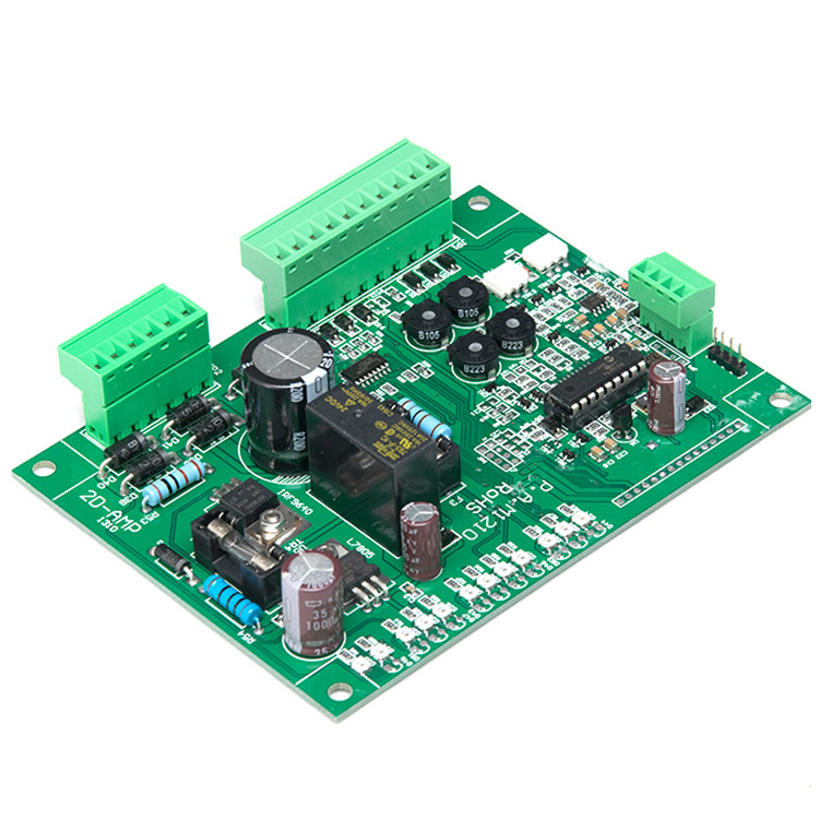
Before the data is released, the design is checked against the manufacturing process rather than only against the schematic. The minimum line width and spacing, the drill sizes and their aspect ratios, the annular ring, the solder mask sliver, the copper to edge clearance and the panel utilisation are all reviewed against what the process can produce repeatedly.
The assembly requirements are reviewed in the same pass. The stencil design for the fine pitch devices and the thermal pads, the fiducials, the orientation markings and the courtyard clearances are checked, because a board that cannot be printed or placed reliably is a board with a hidden cost that appears in the production figures rather than in the design review.
The tests are considered at the same time: the access points, the test pads, the programming interface and the fixture requirements. A test point that would have been free at the layout stage is expensive to add afterwards.
What Is Delivered
The deliverable is not only the artwork. It is a released Gerber set together with the drill data, the stack-up drawing, the bill of materials, the placement coordinates, the assembly drawing, the fabrication notes and the design files in their native format. The set is consistent, so that the fabricator and the assembly house are working from the same revision, and the notes state the finish, the impedance requirements and the tolerance of the profile.
That consistency is the practical difference between a design that moves into production and a design that generates a week of correspondence. The same team can also take the design forward through PCB manufacturing, SMT assembly, component procurement and PCBA testing, which removes the handover that most often loses the information a later stage needs.
Working With an Existing Design
A large share of design work starts from something that already exists, and the first task in that case is to establish what can be trusted. A schematic inherited from another supplier may be complete and correct, or it may have been edited outside the design tool, or it may describe a revision that was never built. Until that question is settled, any layout work on top of it is built on an assumption.
The review therefore begins with the netlist and the component data rather than with the appearance of the drawing. The pin assignments are checked against the datasheets, the package variants are confirmed against the physical parts, and the supply and reset sequences are traced through the circuit. Where the original documentation is incomplete, the missing information is reconstructed and confirmed with the customer instead of being inferred.
Once the design is understood, the second question is whether it should be reproduced as it stands or improved. There is a real cost to changing a design that already works, and there is also a real cost to reproducing a design that carries an expensive component or a layout that cannot be manufactured economically. The two positions are compared on evidence, and the decision belongs to the customer with the trade-offs stated plainly.
A Gerber set from an existing product is also useful as a reference even when it is not published: the pad geometry, the stack-up and the finish recorded in the fabrication notes tell the design team what the previous route was capable of, and whether the new design should stay inside those limits or move to a different class.
The same reasoning applies to a layout that is inherited without its design rules. Rebuilding the rules from the artwork is a small task that removes a large risk, because a board that was drawn to a different set of constraints will produce violations that are only visible once the correct rules are applied. Our PCB capabilities page defines what those rules should be for the process the board will be built on.
FAQ
Can a layout be done from an existing schematic? Yes. A schematic supplied by the customer is reviewed against the component data and the manufacturing capability first, and any conflict is raised before the layout begins.
How is the design checked before release? Against the circuit, against the component data and against the process capability, in three separate passes rather than one.
What is included in the delivery? The Gerber set, the drill data, the stack-up, the bill of materials, the coordinates, the assembly drawing, the fabrication notes and the native design files.