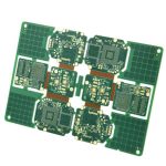
EMC Design for PCB Layout
EMC Starts on the Board
Electromagnetic compatibility is usually treated as a test that happens at the end of a project, and by then most of the cost is already committed. The behaviour that the test measures is decided by the layout: the size of the loops that carry the switching currents, the continuity of the return paths, the placement of the filters and the arrangement of the connectors. A product that fails its emission test is usually a product whose layout allowed a current to return by a path other than the one intended. Correcting that after the boards are made is expensive, and designing for it from the start is not.
Return Paths and Loop Area
Every signal current returns to its source, and at high frequency it returns by the path of least inductance, which is the plane directly beneath the trace. Where the plane is continuous, the loop is small and the field is confined; where the plane is split, the return current has to divert, and the resulting loop is large and radiates. The same logic applies to a power and ground pair: the closer they are, the smaller the loop between them and the lower the radiated field. Keeping the return path continuous, and never routing a fast signal across a split in its reference plane, is the single most effective EMC measure in a layout.
Grounding and the Reference
The ground is a reference and a return, and treating it as a single point that is the same everywhere is the error that produces most EMC problems. The currents flow through the plane, and the voltage developed across the plane’s impedance appears between the different points that the circuit assumes are the same. A connector at one end and a filtered circuit at the other will see a different ground, and the difference drives current through the shield or the cable. The layout should therefore plan where the currents flow in the plane, and should avoid forcing a large current through a part of the plane that the sensitive circuits share.

Filtering and Decoupling
The decoupling capacitor has to be placed where it acts, which is between the pin and the plane with the shortest possible loop. A capacitor a centimetre away has an inductance that makes it ineffective at the frequencies that matter. The same applies to the filters on a connector: a filter placed away from the connector allows the current to radiate from the trace between them before the filter removes it. The filter’s return should be to the plane directly beneath, so that the loop is small. Where a common mode choke is used, its placement and its return determine whether it works.
Cables and Connectors
A cable is an antenna, and the current that flows on it comes from the ground of the board. Where a board’s ground is driving a cable, the cable radiates. The countermeasures are to keep the ground quiet at the connector, to filter the signals that leave the board, to provide a low impedance connection to the chassis where one exists and to keep the common mode impedance of the cable as high as possible. Where the board is inside a metal enclosure, the connector’s screen should be bonded to the enclosure, and the bonding should have a low impedance at the frequencies of interest rather than only at dc.
Clock, Switching and Layout Discipline
The largest sources are the switching supplies, the clocks and the fast digital buses. The switching supply’s hot loop should be minimised, its input filter placed at the source of the current, and its inductor oriented so that its field does not couple into the cables. A clock should be routed with a continuous return, terminated where the frequency requires it, and kept away from the connectors and the edges. A fast bus should be routed over a plane, with its return adjacent, and its edge rates kept no faster than the timing requires. These are layout measures and they are cheaper than a shielding solution.
Verification
The layout should be verified before the formal test. A near field probe scan of a prototype board shows where the field is concentrated, and a spectrum analyser on the cables shows the common mode current, both of which identify the offending loop. A pre-compliance measurement in a screened room gives a result close enough to the formal test to allow a correction before the cost of the formal test is incurred. Where a failure occurs, the diagnosis should identify the loop or the cable that carries the current rather than a component, because the component is usually a symptom and the loop is the cause.
Design Reviews for EMC
An EMC review is most useful at the layout stage, when the loops and the returns can still be changed. The review should ask where each high current loop closes, whether any fast signal crosses a split in its reference plane, whether the filters are at the connectors, and whether the cables are driven by a quiet ground. Those questions can be answered from the layout data, and a negative answer identifies a change that costs a routing edit rather than a new board. Adding the review to the existing design review costs an hour and saves the schedule that a failed test would consume.

FAQ
Why does the return path matter so much? Because the return current forms the other half of the loop, and a diverted return makes the loop large and radiating.
Why is decoupling placement critical? A capacitor that is remote has inductance in its connection, which makes it ineffective at the frequencies that matter.
What makes a cable radiate? A current on the cable’s ground, driven by the board’s ground impedance or by a common mode voltage.
Where should a filter be placed? At the connector or the pin, so that the current cannot radiate from the trace before it is filtered.
How can a design be checked before the formal test? With a near field scan and a pre-compliance measurement on a prototype.
Conclusion
EMC is decided by the loops and the return paths, so design them deliberately and place the filters where they act. Check the prototype before the formal test. EMC layout belongs to PCB design and layout, the stackup that supports the return is described under PCB capabilities, and the verification is part of PCBA testing. EMC critical designs are first built during prototype PCB assembly in 2026.