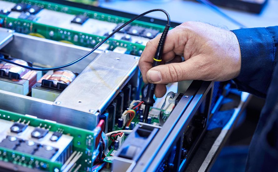
Grounding Strategy for Mixed Signal Boards
The Question and the Argument
Grounding a mixed signal board is one of the most argued topics in layout, because both of the common answers can be defended. One camp splits the plane into an analogue part and a digital part and joins them at one point; the other uses a single continuous plane and relies on placement to keep the currents apart. Both approaches work when they are implemented with the currents in mind, and both fail when they are applied as a rule without understanding. The useful way to decide is to understand where the return currents flow, and to make the layout agree with that.
How Return Current Flows
A signal current returns to its source by the path of least impedance. At low frequency that is the path of least resistance, which may be a long way round; at high frequency it is the path of least inductance, which is the plane directly beneath the trace. The transition between the two regimes happens at a frequency that depends on the geometry, and for most digital signals the high frequency behaviour dominates the edges. The consequence is that a trace’s return is beneath it, and that placing a barrier across the return path forces the current to divert, which increases the loop and radiates.
The Case for a Continuous Plane
A continuous plane gives every trace a return path directly beneath it, so the loops stay small and the fields stay confined. The analogue and the digital circuits then have to be separated by placement rather than by copper: the analogue components go in one area, the digital in another, and the converter sits at the boundary with its analogue pins facing the analogue side. The advantage is that no signal ever crosses a gap, and the disadvantage is that the analogue reference is shared with the digital, so the placement has to be disciplined.

The Case for a Split
A split plane prevents the digital return current from flowing through the analogue reference, and it is the traditional approach for a converter with a separate analogue and digital ground pin. Its risk is that a signal routed across the split creates a large loop, so the split must be arranged so that no signal crosses it except at the single connection point, and that requires the routing to respect the boundary. Where the converter’s data interface must cross the boundary, a bridge or a specific crossing point is provided, and the interface is arranged so that the return crosses with it.
Making Either Work
The two approaches converge on the same requirement: the digital return current must not flow through the reference that the analogue circuit uses. Whether the plane is continuous or split, the layout has to place the components and route the signals so that this is true. In a continuous plane, that means physical separation and careful routing; in a split plane, it means respecting the boundary and crossing only at the join. The failure mode is the same in both cases: a fast digital return flowing through the analogue area, and the analogue performance degrading in a way that no component change will fix.
Slots, Stitching and the Plane’s Impedance
A plane is not a perfect conductor, and its impedance develops a voltage between two points as current flows. A large current in one area raises the potential there relative to another area, which appears as a difference between circuits that assume a common reference. The countermeasures are to keep the large currents away from the sensitive area, to keep the plane’s impedance low by using a solid plane rather than a hatched one, and to place the decoupling where the currents are. Stitching vias between the ground layers reduce the impedance and confine the current, and their placement should follow the current rather than a uniform grid.
Practical Rules
The rules that emerge are simple and worth writing down. Keep the return path continuous under every fast signal. Do not route a signal across a split in its reference unless the return crosses with it. Define the analogue and the digital areas and place the components accordingly. Put the converter at the boundary with its pins facing the correct side. Keep the switching supplies and the large currents away from the analogue area. Use a solid plane for the reference. And verify with a measurement of the analogue performance rather than with an inspection of the layout.
Grounding at a Connector
The connector is where the board’s ground meets the outside world, and it is the point at which a difference in potential becomes a current on a cable. The ground at the connector should be quiet, which means the large currents should not flow through that part of the plane, and the shield, where there is one, should be bonded to the chassis with a low impedance at the frequencies of interest. Where the connector carries signals that leave the board, their filters should return to the same point rather than to a remote part of the plane, so that the filtered current does not travel along the cable’s ground. The connector’s ground arrangement is therefore a deliberate part of the grounding strategy rather than a detail of the mechanical design.
FAQ
Should the ground plane be split? Either approach works if the return currents are respected; the choice depends on the converter and the routing.
Why does a signal crossing a split matter? The return current has to divert, which makes the loop large and radiates energy.
Where do high frequency return currents flow? In the plane directly beneath the trace, because that is the path of least inductance.
Why not use a hatched plane? Its impedance is higher than a solid plane’s, so the voltage developed across it is larger.
How is the strategy verified? By measuring the analogue performance and the noise floor, not by inspecting the layout.
Conclusion
Grounding is a question about where the currents flow, so decide the strategy from the return paths and make the placement agree with it. Then measure the result. Ground design belongs to PCB design and layout, the stackup that provides the planes is described under PCB capabilities, and the verification is part of PCBA testing. Mixed signal boards are first built during prototype PCB assembly in 2026.