



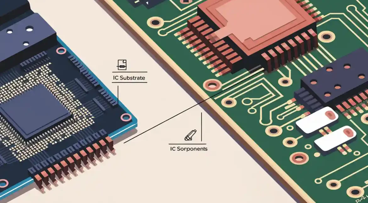
PCB Layout Design Services for High-Speed and HDI Boards
A schematic can be correct and still fail on the bench. The physical layout decides how signals travel, how power reaches each device, and how much noise escapes the board. High-speed and HDI designs raise the stakes because traces are shorter, layers are denser, and vias are smaller. This guide explains what a layout service should deliver, which decisions belong to the engineer, and what a buyer should check before releasing files to production.
Layout work starts with the netlist and the mechanical drawing, not with the router. The engineer must confirm packages, connector positions, board outline, and mounting holes before placing a single part. For HDI boards, the via structure and layer count also constrain placement from the first hour. A layout that ignores these limits will need rework later. Reviewing them early keeps the schedule realistic and the cost predictable for both sides.
What Layout Work Covers
PCB layout converts an electrical schematic into a physical board that meets electrical, mechanical, and manufacturing requirements. The schematic defines what the circuit does, while the layout decides how it behaves in the real product. Good layout protects signal quality, electromagnetic compatibility, power delivery, and thermal performance. It also keeps the board buildable at a sensible cost. For complex products, placement and routing require far more than connecting nets.
Impedance control, reference planes, differential pairs, and return paths all interact. A change in stackup alters impedance, which alters routing rules, which alters length matching. Engineers who treat these as one system avoid late surprises. Buyers should expect the layout team to ask about interfaces, data rates, and enclosure limits before quoting. Those answers shape the stackup and the routing strategy. They also set the review checkpoints that follow.
Stackup and Impedance Planning
For multilayer boards, layer planning is the most important early decision. A typical stackup uses signal layers, ground planes, and power planes in a fixed order. High-speed signals should route next to a continuous reference plane so the return current has a short path. Splitting a plane under a fast trace creates a detour in the return path. That detour raises radiation and crosstalk. The stackup also fixes dielectric thickness, copper weight, and controlled impedance targets.
Impedance should be calculated before critical routing begins. The fabricator must confirm the stackup is buildable with available materials and processes. For HDI, microvia and buried via structures add constraints that affect layer assignment. Fine-pitch BGA escape routing depends on via-in-pad rules and annular ring limits. Engineers should agree these details with the factory early. A stackup that cannot be built to tolerance will fail at the first prototype.
Placement by Functional Block
Placement should follow the functional architecture of the circuit. Group the processor, memory, power supply, interfaces, analog sections, and connectors into clear blocks. Interface circuits belong near their connectors, with ESD protection in the correct position along the signal path. Decoupling capacitors belong close to the pins they serve. This order keeps signal paths short and logical. It also makes the board easier to review and debug.
Separation matters as much as grouping. Switching supplies, clock circuits, and high-current devices generate noise that can couple into sensitive analog or RF sections. Physical distance and appropriate grounding reduce that coupling. Analog and digital blocks should be placed with their return currents in mind. A layout that looks tidy but mixes noisy and sensitive circuits will still fail EMC testing. Placement review before routing is the cheapest place to fix this.

Power Delivery and Grounding
Power distribution is a core layout task, not an afterthought. The main supply should sit near the power entry point, with local regulators close to the loads they feed. High-current paths need short, wide copper to limit voltage drop and impedance. The full current loop matters for EMC, because a large loop behaves like an antenna. Keeping the loop small reduces radiation. Continuous ground planes support both power integrity and signal return.
Decoupling strategy deserves the same attention. Capacitors must connect to planes with short, low-inductance paths to be effective. A capacitor placed far from the pin does little at high frequency. Power plane design should support current distribution without excessive splits. Grounding should be planned rather than inherited from leftover copper. Buyers should ask how the power delivery network was checked, especially on boards with many rails and tight voltage margins.
High-Speed Routing and Matching
High-speed routing controls effects that barely matter at low frequency. Impedance, propagation delay, crosstalk, reflections, and via transitions all affect signal quality. Interfaces such as PCIe, USB, SATA, and high-speed Ethernet need controlled routing and continuous reference planes. Every via adds a discontinuity, so layer changes should be planned rather than casual. Termination strategy should match the interface requirements. These choices should follow the stackup and the simulation results.
Differential pairs need consistent width, spacing, and reference. Length matching should follow the specified tolerance for the interface, not a blanket rule. Skew within a pair matters as much as total length. Timing differences on a high-speed bus can degrade performance even when every trace looks neat. Engineers should route critical groups first and check them before general routing. A layout service that can show its impedance and matching reports is easier to trust during prototype debug.
Signal and Power Integrity Checks
Simulation helps find problems before prototypes are built. Signal integrity analysis covers impedance, reflections, crosstalk, timing, and eye diagrams for critical nets. Power integrity analysis covers plane design, decoupling, current distribution, and voltage stability. Not every net needs simulation, so the engineer should select the critical ones. Early analysis reduces redesign risk and prototype iterations. It also gives the buyer evidence that the layout was verified, not just drawn.
EMC should be designed in from the start. Keep high-speed traces short, maintain continuous reference planes, and minimize current loops. Separate noise sources from sensitive circuits and place filtering components correctly. Avoid unnecessary layer changes and trace crossings. A layout that handles EMC early is cheaper than one that needs shielding or rework after a failed test. Buyers should confirm that EMC review is part of the layout scope, not a separate purchase later.
HDI, Flex, and Rigid-Flex Layout
HDI design uses microvias, blind and buried vias, and fine-pitch routing to raise component density. The layout must coordinate stackup, via structure, BGA escape routing, impedance, and manufacturing process. Via-in-pad and filled via choices affect assembly yield, so they should be agreed with the fabricator. Fine lines and spaces push etching tolerances, which changes the design rules. Engineers should confirm the factory capability before routing dense areas. HDI savings come from density, not from ignoring process limits.
Flexible and rigid-flex boards add mechanical constraints to the electrical ones. Bend areas need careful copper routing, defined bend radius, and suitable stiffeners. Copper in a bend should run in a direction that tolerates flexing. Connector transitions and stiffener edges create stress points that deserve review. These boards also need clear fabrication drawings so the factory builds the right construction. Buyers should ask how bend areas were checked and whether the mechanical drawing matches the layout.

Workflow and Verification
A structured workflow keeps layout quality predictable. It starts with the schematic, netlist, BOM, mechanical drawing, and design requirements. Engineering review then confirms scope, complexity, and stackup before placement begins. Preliminary placement is reviewed with the customer before detailed routing. Critical signals are routed first, followed by other groups. The completed layout then goes through design rule checks, DFM review, and EMC review. Final output includes source files, Gerber, drill, and assembly data.
Production files should be checked against the fabrication and assembly process. Design rule violations, clearance issues, and component placement errors should be closed before release. If the project also needs PCB design and layout support from schematic capture onward, the same review steps apply. Many teams combine layout with PCB assembly so that fabrication and placement data are checked together. That reduces handoffs and catches mismatches between the layout and the assembly drawing.
For prototypes, SMT PCB assembly feedback often reveals pad or stencil issues that layout can correct before volume.
Buyer Checks Before Release
Before approving a layout, confirm the stackup, impedance targets, and layer count with the fabricator. Check that critical nets have documented routing rules and matching tolerances. Ask for the design rule report and the DFM findings. Confirm that connector positions and mounting holes match the mechanical drawing. Review the assembly data, including polarity and reference designators. These checks take little time and prevent costly rework.
For projects moving to volume, plan PCBA testing coverage alongside the layout review. Test points and access need space on the board, and adding them late is expensive. If the supply chain spans several suppliers, turnkey PCB assembly can keep fabrication, sourcing, and assembly under one schedule. The layout should also record which revision was released and what changed. That record is the fastest way to trace a field issue back to a design decision.
The practical takeaway is simple. Treat stackup, placement, and routing rules as one agreed package before detailed routing starts. Ask for the impedance plan, the design rule report, and the DFM findings in writing. Confirm that test access and assembly data match the layout revision. A layout service that documents these steps gives the buyer a board that can be built, assembled, and tested without surprises at the prototype stage.