Where Signal Integrity Begins in PCB Manufacturing
Signal integrity is often treated as a design problem alone. In practice, the board that leaves the factory decides whether the design works. Trace width, dielectric thickness, copper roughness and layer alignment all shift during fabrication. Each shift moves impedance away from the value the engineer calculated. Precision PCB manufacturing is the discipline that keeps those shifts inside a controlled window. This article explains where signal quality is won or lost on the production floor.
Buyers and engineers should read the same evidence. A quotation that lists only layer count and finish hides the process controls that matter. Ask instead how impedance is measured, how stackups are locked, and which records travel with the lot. Those answers separate a supplier that can repeat a build from one that can only sample it. The sections below follow the board from material selection through electrical test, with the checkpoints that deserve review before release.
Material Choice Sets the Baseline
Substrate properties define how a signal behaves before any copper is etched. Dielectric constant controls propagation delay and impedance. Loss tangent controls attenuation at higher frequencies. Thermal and moisture behavior decides whether those values stay stable over the product life. A material chosen only on price can meet the drawing at first article and drift later. Engineers should confirm the laminate family, the glass style and the resin content against the actual data sheet.
Material verification is a buying checkpoint, not a formality. Ask for the laminate supplier, the lot traceability and the certificate of analysis for the batch used. Confirm that the dielectric thickness assumed in the stackup matches what the fabricator will press. When a substitute is proposed, check its electrical values against the original before approval. A small change in dielectric constant moves impedance, and that change reaches every high-speed net on the board.
Trace Geometry and Copper Control
The trace is the transmission path, so its dimensions carry the signal. Width, thickness and cross-section determine impedance and resistance. Etching removes copper from the sides as well as the top, so a wide trace becomes narrower than drawn. Fabricators compensate in the artwork, but the compensation depends on copper weight and etch conditions. Precise imaging and controlled etch lines keep that compensation predictable across panels and across lots.
Layer-to-layer registration matters just as much. A drilled via that lands off center adds stub and changes the return path. Misregistration between a signal layer and its reference plane changes the distance that sets impedance. Buyers should ask how registration is measured and what tolerance the factory holds. The answer should reference a measurement on the panel, not a machine specification. PCB design and layout decisions set the target, but only fabrication control holds it.
Impedance Control in Production
Impedance control links the design calculation to the physical board. The fabricator builds a test coupon alongside the panel and measures it. That coupon reflects the same line width, dielectric thickness and copper distribution as the product. If the coupon passes, the panel is likely to pass. The value of the method depends on the coupon being representative and on the measurement being recorded. Ask which coupon design is used and how often it is checked.

Several variables move impedance during a run. Dielectric thickness varies with press pressure and prepreg flow. Trace width varies with etch. Solder mask adds a thin dielectric layer over the trace. A capable factory controls these variables and reports the measured result. When a lot drifts outside the window, the cause should be identified before the next build. That closed loop is what makes impedance repeatable rather than lucky.
Stackup Decisions That Hold
The stackup is where electrical intent becomes a manufacturing plan. Signal layers need reference planes close by. Power and ground pairs need the right dielectric separation. Symmetric construction reduces warp during lamination. Each of these choices affects impedance, crosstalk and radiation. A stackup that looks fine on paper can fail in the press if prepreg availability forces a substitution. Locking the stackup early prevents that surprise.
Engineers should review the stackup with the fabricator before tooling. Confirm the dielectric thickness for each signal layer and the copper weight on each plane. Check that the reference plane under a high-speed net is continuous. Ask how the factory handles any change forced by material availability. A written stackup with agreed limits gives both sides a fixed target. It also gives the inspector something concrete to verify on the finished board.
Drilling, Plating and Via Quality
Vias carry high-speed signals between layers, so their quality affects loss and reflection. Drill registration, hole wall roughness and plating thickness all contribute. A rough wall increases loss at high frequency. Thin plating can crack under thermal cycling. Backdrilling removes unused via stubs that cause reflections, but it adds process steps and needs its own control. Each of these points should appear in the process plan for any high-speed design.
Ask how the factory verifies hole quality. Cross sections show wall roughness and plating thickness on a sample. Continuity and isolation tests catch opens and shorts across the panel. For dense designs, via reliability under thermal stress deserves a review before volume release. These checks are routine for a capable fabricator and should be documented. When they are missing from the process description, the buyer is carrying the risk.
Surface Finish and Long-Term Contact
Surface finish protects the copper and provides a solderable surface. It also affects high-frequency loss, because some finishes are more lossy than bare copper. ENIG offers a flat surface and good shelf life. HASL is economical but leaves uneven topography. OSP is simple and flat but has a short window. Immersion silver and tin each have their own tradeoffs. The right choice depends on frequency, assembly process and storage time.
Finish thickness and uniformity need control. Thin immersion gold over nickel can leave porosity and corrosion sites. Uneven finish can cause solderability problems at assembly. Buyers should confirm the finish specification, the thickness target and the inspection method. For long-life products, the finish should match the storage and operating environment. A finish chosen only for cost can create field returns that cost far more than the difference.
Process Control and Test Coverage
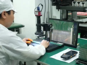
Signal integrity depends on the whole chain, not on one step. Lamination, drilling, plating, etching and finishing each feed the next. A parameter that drifts at one stage shows up as a defect several stages later. Factories that record process data can trace a failure back to its cause. Factories that do not simply repeat the same mistake. The record is what turns a capable line into a predictable one over many lots.
Electrical test closes the loop. Impedance coupons confirm the target. Continuity and isolation tests catch opens and shorts. Functional test confirms the assembled board under power. For critical products, thermal cycling and burn-in add confidence. These steps connect naturally to PCB assembly, where the same records guide placement and reflow. A buyer who reviews test coverage before release avoids surprises after the first shipment.
What Buyers Should Verify
Before placing an order, confirm the material, the stackup and the impedance target in writing. Ask how each is measured and which records ship with the lot. Review the first article against those numbers rather than against a picture. Check that any substitution passes through an approval step. These questions cost little at the start and prevent rework later. They also make supplier comparison concrete instead of subjective.
For projects that move to volume, plan the handoff early. Turnkey PCB assembly and high-volume PCB assembly both depend on a stable bare board, so fabrication control protects the whole build. Component procurement should start once the design is frozen, because part changes can force layout changes. Keep the approved stackup and the impedance report with the project file. That file is the fastest way to resolve a field question months later.
The practical takeaway is simple. Signal integrity begins where the design meets the process. Lock the material and stackup, measure impedance on every lot, and keep the records with the boards. Ask suppliers for those records before you compare prices, because a low quote without process data carries hidden cost. Precision is not a claim in a brochure. It is a measured value on a coupon, repeated across builds.