PCB Profiling: Routing, V-Score and Punching
What Profiling Does
Profiling is the step that separates the individual boards from the panel. It is one of the last operations in fabrication and one of the most consequential, because it sets the edge quality, the mechanical strength of the edge, the tolerance on the outline and the amount of panel area that is consumed by rails and tabs. The three common methods are routing with a milling bit, V-scoring with a circular blade and punching with a hard tool. Each has a range of board thickness, edge complexity and volume where it is the right answer.
Routing with a Milling Bit
Routing cuts the outline with a small carbide bit running at high speed, following the board contour. It can follow any shape, including internal cut-outs, curved edges and slots, and it can cut a fine set of tabs that hold the board in the panel until final assembly. The edge is a machined edge with a slight tool mark, and the tolerance is set by the machine and the bit rather than by the artwork. Routing suits low and medium volume, complex outlines and rigid-flex work, and it is the only practical method for internal features that are not a straight line.
V-Scoring
V-scoring runs a blade along both sides of the panel to cut a V-shaped groove, leaving a thin web of material to hold the panel together. The boards are snapped apart at assembly. The method is fast and cheap on straight-line boards with rectangular outlines, and it consumes almost no panel area. Its limits are rigid: the outline must be a straight line across the panel, the remaining web must be sized to the board thickness, and the boards must be rectangular. The cut also leaves a visible V groove on the edge, which matters for some connectors and for boards that must fit a tight enclosure, and the snapping operation leaves a small burr and a slight dimensional variation along the edge.
Punching
Punching uses a hard tool, usually a steel die, to shear the outline in a single press stroke. It is the fastest method per board and gives excellent repeatability once the tool exists, which makes it ideal for high volume consumer work on thin, simple boards. The cost is entirely in the tool, which is specific to one outline, and the method is unforgiving about thickness, material and internal features. It also puts mechanical stress into the panel, so it is normally used on thinner boards and on outlines without delicate features near the edge.
Edge Quality and Tolerance
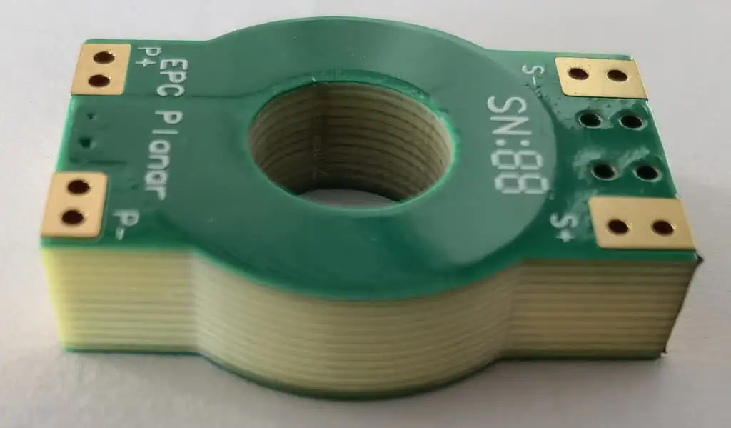
A routed edge has a machined texture and a tolerance in the region of a few tenths of a millimetre. A V-scored edge is defined by the blade geometry and by how the panel breaks, so the edge is not a clean vertical wall and the dimensional result varies along its length. A punched edge is the most repeatable in dimension but can show a shear band and slight distortion. Where the board edge carries a plated feature, such as an edge connector or a castellation, the tolerance that matters is the one the plating process can hold, and the profiling method has to be chosen so that it does not damage the plated surface.
Panel Layout and Utilisation
The choice of profiling method determines how the panel is laid out. V-scoring needs continuous straight lines across the panel, which forces the array into rows and columns and forbids nesting. Routing allows any arrangement and lets a designer nest boards of different shapes. Punching needs a tool with enough clearance for each outline, and the die layout is expensive to change. Where the design has an irregular outline, the cost of the extra panel area that V-scoring cannot use is often larger than the saving in the profiling step, which is a calculation worth doing at the panelisation stage rather than after the tooling is ordered.
Choosing a Method
Start from the outline. If it is a rectangle and the volume is high, punching or V-scoring will be cheaper. If it contains curves, internal cut-outs or different board shapes on one panel, routing is the practical answer. Then check the edge requirement: an edge that must fit a connector or a chassis, or that carries plating, may rule out V-scoring regardless of cost. Finally, check the thickness: very thin boards distort under punching, and very thick boards need a deeper V-groove and a more careful break.
Depanelling and Breakaway Design
The profiling method is only half of the decision, because the tabs and grooves that hold the board in the panel are part of the design. Routed tabs should be placed so that the board is supported through handling and test, and they should not sit where a subsequent process, such as a connector insertion or a coating, will stress the joint. V-score webs should be positioned so that the break leaves no burr on a functional edge, and the board should be oriented so that the break runs away from fine features. Where a board carries heavy components, the direction of the break and the position of the tab determine whether the panel survives assembly at all. A depanelling step that tears the laminate near a plated hole is a design defect rather than a machine fault, and it is cheaper to move the tab on the drawing than to change the process.
FAQ
What is the cheapest profiling method? Punching at high volume, V-scoring at medium volume on rectangular boards. Routing is the most flexible but not the cheapest per board.
Can V-score curved outlines? No. It is limited to straight lines across the panel and to rectangular boards.
How much material does V-scoring waste? Very little, because the groove is narrow and the panel can be fully used in rows and columns.
Which method gives the best edge? Routing gives a machined edge with predictable tolerance; punching gives excellent repeatability; a broken V-score edge is the least uniform.
Can internal cut-outs be punched? Only where the tool is designed for them, and usually only at very high volume, since the die cost is significant.
Conclusion
Profiling is a cost and tolerance decision that has to be made while the panel is being laid out, not after the tooling is ordered. Match the method to the outline, the thickness, the edge requirement and the volume, and check the panel utilisation that the method allows. Panel design and breakaway features belong with PCB capabilities, the final fabrication operations are described in PCB manufacturing, and the tabs and edge clearances are set in PCB design and layout. Depanelling and edge handling continue into PCB assembly in 2026.