PCB Schematic Design Guidelines: PCB Design, PCB Manufacturing & Best Practices
PCB Design is a fundamental part of electronic product development, and a clear, well-organized schematic is at the heart of a successful circuit design. A PCB schematic provides an overview of the electrical system and serves as the foundation for PCB layout, component placement, routing, testing, and manufacturing.
A well-designed schematic is more than a collection of symbols and electrical connections. It acts as a common reference for designers, hardware engineers, firmware engineers, manufacturing teams, and technicians. A clear schematic makes it easier to understand circuit functions, identify design problems, review engineering decisions, and communicate effectively across different departments.
However, simply creating an electrically correct schematic does not necessarily make it easy to read or maintain. Large and complex schematics can quickly become difficult to understand when symbols, connections, labels, and functional blocks are not organized consistently.
This guide explains practical PCB schematic design guidelines for creating professional, readable, and manufacturing-friendly schematics.
1. Organize the PCB Schematic in a Logical Layout
One of the most important principles of PCB schematic design is establishing a clear and logical layout.
A schematic should allow engineers to follow the signal flow and understand the relationship between functional blocks without having to mentally reconstruct the entire circuit.
Use a Left-to-Right and Top-to-Bottom Flow
Whenever practical, arrange the schematic so that the primary signal flow moves from left to right and from top to bottom.
For example, a typical system may be organized as:
Power Input → Power Management → Processing → Interfaces → Outputs
Power inputs can be placed toward the left or upper portion of the schematic, while outputs, communication interfaces, or actuators can be positioned toward the right.
This approach creates a natural visual flow and allows engineers to understand the circuit architecture more quickly.
Group Related Components
Components belonging to the same functional circuit should be grouped together.
Typical functional blocks may include:
- Power supply and voltage regulation
- Microcontroller or processor circuitry
- Memory
- Analog signal conditioning
- Sensors
- Communication interfaces
- Motor or actuator drivers
- Filtering and protection circuits
Clearly separating these blocks makes the schematic easier to review and simplifies troubleshooting.
Avoid Unnecessary Wire Crossings
Excessive wire crossings make schematics difficult to read.
Where possible, route connections cleanly and use net labels instead of long wires when appropriate. Common labels such as GND, VCC, DATA_IN, CLK, RESET, SPI_MOSI, and I2C_SDA can significantly reduce visual clutter.
Wire crossings should not be used merely to make a schematic look compact. Readability should always take priority.
2. Use Standardized Symbols and Naming Conventions

Consistency is essential when creating a professional PCB schematic.
Standardized symbols and naming conventions allow different engineers and manufacturing personnel to interpret the design consistently. Widely recognized electrical symbols are defined by industry standards such as IEEE 315 and IEC 60617.
Follow Industry-Standard Symbols
Use conventional symbols to represent resistors, capacitors, inductors, diodes, transistors, integrated circuits, connectors, and other electrical components.
Avoid using arbitrary symbols that may cause ambiguity. A symbol should clearly communicate the function and electrical characteristics of the component.
Use Consistent Reference Designators
Every component should have a unique reference designator.
Typical examples include:
- R1, R2, R3 for resistors
- C1, C2, C3 for capacitors
- L1, L2 for inductors
- D1, D2 for diodes
- Q1, Q2 for transistors
- U1, U2 for integrated circuits
- J1, J2 for connectors
Reference designators should remain consistent throughout the schematic and PCB layout.
Use Meaningful Net Names
Net names should communicate the function of the associated signal.
Instead of using generic names such as “Net1” or “Wire1,” use meaningful names such as:
- VCC_5V
- VCC_3V3
- GND
- RESET
- CLK
- DATA_IN
- DATA_OUT
- USB_D+
- USB_D-
- SPI_MOSI
- SPI_MISO
Meaningful net names make schematic review, PCB layout, debugging, and manufacturing documentation much easier.
3. Clearly Identify Power and Ground Networks
Power and ground are fundamental to almost every electronic circuit. They should therefore receive special attention during PCB Design.
Poorly organized power connections can make a schematic confusing and can also make it more difficult to verify the power architecture.
Use Consistent Power Symbols
Use consistent symbols and naming conventions for power networks.
For example, a design may use:
- VCC
- 5V
- 3.3V
- VDD
- GND
However, different voltage domains should not be given ambiguous or interchangeable names.
If multiple power domains exist, use descriptive names such as 1V2, 1V8, 3V3, 5V, or AVDD to clearly distinguish them.
Use Global Power Labels Where Appropriate
Long power and ground wires can unnecessarily clutter a schematic.
Power symbols and net labels can provide logical connections without requiring every power connection to be physically drawn across the page.
This makes the schematic cleaner and easier to review while preserving electrical connectivity.
Place Power Toward the Top and Ground Toward the Bottom
A common schematic convention is to place power-related circuitry toward the top and ground symbols toward the bottom.
For example:
Power Input → Regulator → Functional Circuit → GND
This convention is not an electrical requirement, but it provides a familiar visual hierarchy that makes the schematic easier to understand.
4. Add Annotations and Design Documentation
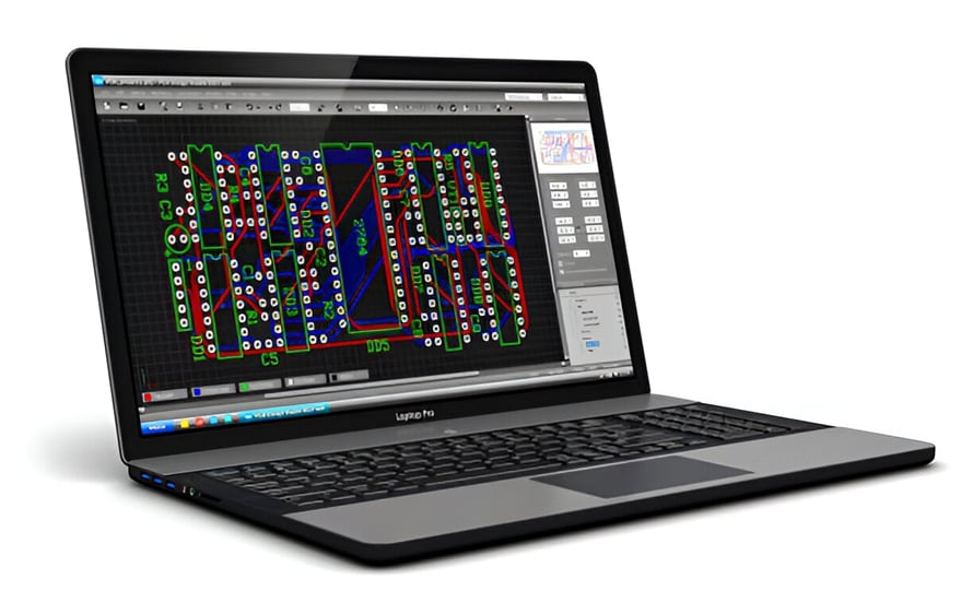
A technically correct schematic can still be difficult to understand if it lacks sufficient documentation.
Adding concise notes, descriptions, and design comments helps other engineers understand why particular components or circuits were selected.
Add Explanatory Notes
Important or complex circuit sections should include short descriptions.
For example:
- “C5 provides local high-frequency decoupling.”
- “Q2 is used as a high-side switching device.”
- “R8 provides the required pull-up for the I2C bus.”
- “U3 converts the input voltage to a regulated 3.3 V rail.”
These notes reduce the amount of reverse engineering required during design reviews and troubleshooting.
Include Component Values
Component values should be clearly defined.
For example:
- Resistors should include resistance values.
- Capacitors should include capacitance values.
- Inductors should include inductance values.
- Diodes should identify the appropriate part number where necessary.
- ICs should include complete part numbers or manufacturer part information.
Component values are particularly important when the schematic is transferred to the BOM and manufacturing documentation.
Document Important Design Decisions
If a component value or circuit topology was selected for a specific engineering reason, document that decision.
For example, if a particular pull-up resistor value was selected because of signal rise-time requirements, adding a short engineering note can help future engineers understand the original design intent.
This becomes especially valuable when the PCB is revised months or years after the original design.
5. Use Hierarchical Schematics for Large Designs
As circuit complexity increases, placing every component on a single schematic sheet can quickly become impractical.
A hierarchical schematic structure divides a large design into smaller functional sections while maintaining logical connections between them.
Divide the Design into Functional Modules
A large PCB schematic can be separated into dedicated functional sheets, such as:
- Power supply
- Microcontroller
- Memory
- Analog circuitry
- Sensor interface
- USB interface
- Ethernet
- Wireless communication
- Motor control
- External connectors
Each sheet should represent a meaningful functional block rather than an arbitrary collection of components.
This approach makes the design easier to navigate, review, modify, and troubleshoot.
Use Hierarchical Ports and Off-Sheet Connections
When signals must pass between schematic sheets, use clearly named hierarchical ports or off-sheet connectors.
For example, a microcontroller sheet may contain:
SPI_CLK
while the corresponding peripheral sheet uses the same signal name.
Consistent naming ensures that engineers can immediately understand how the functional blocks are interconnected.
Keep Each Sheet Focused
Avoid placing too many unrelated circuits on the same schematic page.
A good hierarchical structure allows engineers to answer questions such as:
- Where does the power come from?
- Which circuit controls this sensor?
- Where is the communication interface?
- Which components belong to the processor?
- Where is the protection circuit?
This significantly improves the usability of complex PCB documentation.
6. Maintain Appropriate and Consistent Spacing
The spacing between symbols, wires, labels, and functional blocks has a major effect on schematic readability.
An overcrowded schematic can make even a simple circuit appear complicated.
Leave Enough Space Between Components
Components should not be placed too close together.
Provide enough space for:
- Net labels
- Component values
- Reference designators
- Signal names
- Design notes
- Connection lines
Adequate spacing also makes future schematic modifications easier.
Use a Consistent Grid
Most modern schematic capture tools provide grid-based placement.
Using a consistent grid helps align symbols, wires, ports, and labels. Proper alignment creates a cleaner schematic and reduces accidental connection errors.
Prevent Text and Wires from Overlapping
Reference designators, component values, and notes should not overlap wires or component symbols.
For example, avoid placing a resistor value directly over a connection line or positioning a reference designator where it can be confused with a net label.
Clear separation between graphical elements and text makes the schematic much easier to interpret.
Additional PCB Schematic Review Checklist
Before releasing a schematic for PCB layout or PCB Manufacturing, engineers should perform a systematic review.
Electrical Checks
Verify that:
- All power pins are correctly connected.
- Ground connections are complete.
- Unused IC pins are handled correctly.
- Signal directions are logical.
- No unintended short circuits exist.
- Critical interfaces use the correct signal names.
- Component values are correct.
Documentation Checks
Verify that:
- Every component has a reference designator.
- Component values are complete.
- Important design decisions are documented.
- Functional blocks are clearly labeled.
- Net names are meaningful.
- Connector pin definitions are clear.
- The schematic is organized consistently.
Manufacturing Checks
Before transferring the design to PCB layout and manufacturing, confirm that:
- The schematic is synchronized correctly with the PCB layout.
- The BOM contains the required component information.
- Manufacturer part numbers are correct where required.
- Component footprints are assigned appropriately.
- Design constraints are defined.
- Critical components and interfaces have been reviewed.
A clean schematic can significantly reduce misunderstandings between design and manufacturing teams.
Why a Professional PCB Schematic Matters
A PCB schematic is not simply a preliminary drawing that exists before PCB layout. It is an important engineering document that records the electrical architecture and design intent of the product.
A well-organized schematic provides several benefits:
- Faster design reviews: Engineers can understand functional blocks more quickly.
- Simpler troubleshooting: Clear signal paths make it easier to trace faults.
- Better collaboration: Hardware, firmware, test, and manufacturing teams can work from a common reference.
- Improved PCB layout: A logical schematic provides a clearer foundation for component placement and routing.
- More efficient manufacturing: Accurate design documentation reduces communication problems during production.
- Easier future revisions: Engineers can understand the original design intent when modifying the product later.
For professional electronics development, schematic quality should therefore be treated as an important part of the overall PCB Design process.
Conclusion
Creating a clear and professional PCB schematic requires more than placing components and connecting wires. The schematic should communicate the circuit’s architecture, signal flow, functional relationships, and design intent as clearly as possible.
The most important principles include organizing the schematic logically, using standardized symbols and naming conventions, clearly identifying power and ground networks, documenting important design decisions, using hierarchical structures for complex projects, and maintaining consistent spacing between graphical elements.
A well-documented schematic also provides a strong foundation for PCB layout, BOM generation, testing, assembly, and PCB Manufacturing. For complex electronics projects, investing time in schematic organization during the early design stage can reduce troubleshooting effort and improve communication throughout the product lifecycle.
At Kingda, a structured engineering approach to PCB design and manufacturing helps ensure that electrical requirements, layout considerations, manufacturing requirements, and documentation remain aligned throughout the development process.