PCB X-ray Inspection of BGA Voids: Seeing Inside the Solder
Modern electronics depend on boards that are assembled correctly the first time. Every product – a phone, a charger, a medical instrument or an industrial controller – relies on thousands of solder joints that must conduct current for years. This article explains PCB X-ray inspection of BGA voids in plain language: what it is, why it matters in finding voids inside a solder joint, and how a contract PCBA factory keeps it under control so that products ship without surprises.
Common Questions
Can the process handle small batches?
Yes. The setup for finding voids inside a solder joint is the same whether the lot is five panels or five hundred, so the tooling is shared and the unit price stays sensible.
How tight can the tolerance be?
It depends on the feature and the material. The rule is to hold the tolerance that the product needs and to leave the rest at a commercial level rather than paying for accuracy nothing uses.
What happens if something is unclear in the file?
An engineering question is raised before tooling. Answering it costs a message; building on a guess can cost the lot.
Understanding PCB X-ray Inspection of BGA Voids
The X-ray passes through the package and the solder, and the dense metal appears dark while the voids appear light.
Why It Matters
A joint with too much voiding runs hot and cracks, and the fault cannot be seen from the outside.

Assembly Steps in Practice
The result depends on the whole chain, not on any single machine. The board design fixes pad sizes and spacing, the printer controls the solder volume, the placement machine positions every component and the reflow oven forms the joints. Each step feeds the next one, which is why SMT PCB assembly should be reviewed as one complete process instead of a collection of separate operations.
Reading It
The void percentage, the size and the position are measured against the limit. The image then decides whether the part passes.
Inspection catches defects before they leave the factory, but its real value is the feedback it gives. When a solder joint fails, the engineer learns whether the paste print, the placement or the reflow profile caused it, and that closed loop between inspection and process control is what pushes defect rates down month after month. Boards that pass visual checks still need electrical verification, because a cracked joint or a wrong component only shows up under power; functional test, in-circuit test and burn in each add confidence, and that is exactly what a structured PCBA testing program delivers.
Reliability does not come from one lucky batch, it comes from repeatability. Parameters are recorded, machines are calibrated, operators are trained, and the same result is produced on Monday and on Friday. Buyers should ask for process documentation, inspection data and test reports, because those records show whether a real quality management system exists in practice or only on paper.
Applications Across Industries
Application experience also matters for manufacturability. A factory that has built similar products for PCB assembly, inspection and quality already knows the typical failure modes, the component pitfalls and the customer questions. That knowledge shortens the DFM review, avoids repeated trial batches and makes the transition from prototype to volume production much smoother for the buyer.
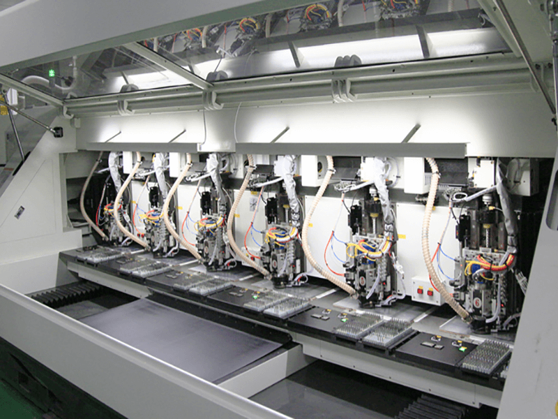
There is more to finding voids inside a solder joint than the machines and materials visible on a factory tour. Temperature and humidity in the assembly area change the behavior of solder paste, and electrostatic discharge can damage sensitive components without leaving a visible mark. Professional factories control these conditions, ground every workstation and store moisture sensitive devices correctly, so the process produces the same result in summer and in winter. These environmental details rarely appear in a quotation, yet they decide whether a line runs at high yield all year or drifts with the seasons.
Documentation matters as much as hardware when it comes to finding voids inside a solder joint. The factory should record which program ran, which reels of paste and components were used, which operator handled the batch and what the inspection found. When a field return arrives months later, that record is the fastest way to identify the cause and to prove that the fix reached the next batch. Buyers should ask for these records as a routine part of every order, because documents that are easy to produce on request are usually also kept honestly during production.
Nothing about finding voids inside a solder joint is decided once and forgotten. Parameters drift, materials change and operators rotate, so the factory reviews its data continuously, ranks the top defects and removes them one by one. Factories that follow this discipline gradually lower their defect rates and shorten their lead times, while factories without data simply repeat the same mistakes at the same cost. The improvement review should happen at least monthly, with the same attendees and the same metrics, so progress stays visible and no problem waits for a crisis to be fixed.
The best factories treat finding voids inside a solder joint as a system rather than a checklist. Every decision, from stencil cleaning frequency to test coverage, connects to the others, so a change in one area is checked against its effect on the rest. A faster placement speed may save time today and create tombstoning tomorrow, and a thicker stencil may fix opens while causing bridges. That systems view, supported by data from inspection and test, is what turns a capable line into a predictable one over years of production.
Communication decides how well finding voids inside a solder joint matches the product intent. When the buyer shares the operating environment and the reliability target, and the factory answers with concrete process choices and test plans, small process changes are approved before they become quality incidents. Regular reporting during production keeps both sides aligned from prototype to volume, and a written summary of every change gives both parties a record they can trust at the end of the program.
Collecting data about finding voids inside a solder joint pays for itself quickly. Print reports, placement statistics, oven profiles and test results cost little to record, yet they turn arguments into decisions: when a customer complains, the batch record shows what actually happened, and when a process drifts, the trend line reveals it before scrap grows. Factories that treat records as part of the process rather than paperwork tend to find problems while they are still cheap to fix, and their customers see the difference in delivery performance and defect rates over time.
A dedicated line only pays for itself when it runs constantly, and keeping process data, calibration records and quality documentation current takes engineering time that is easy to underestimate. Most product companies therefore choose a partner that spreads its equipment investment over many customers and offers services such as high volume PCB assembly and PCB assembly under one roof.
When factories are compared, the price per board should never be the only number. Process controls, inspection equipment, component sourcing and communication decide the real cost, and a partner that reviews files before production, reports risks honestly and keeps its delivery promises will always be cheaper in the long run than one that quotes low and surprises later.
gopcb runs SMT lines supported by solder paste inspection, automated optical inspection and functional test in one facility. Our engineers review your Gerber files and BOM before production, discuss the process options, and ship boards with test records that give you confidence in the field.
If you are planning a new product or moving an existing design to volume production, send gopcb your design files and requirements. You will receive a DFM review, a clear quotation and a schedule you can plan around – and boards that work the way they should.