Planar Coil PCB Design for Inductive Sensing and Power
Some boards exist to carry components, and some exist to be the component. A planar coil replaces a wound inductor with copper windings etched into the layers, and the reason to do that is repeatability as much as size.
What a Coil Board Is
A coil board is a printed circuit board whose copper pattern is drawn as a winding rather than as a network of signal traces. The turns are produced by the same etching process as any other conductor, so the geometry is defined by artwork rather than by a winding machine.
That gives a repeatable inductance from unit to unit, no assembly step, a very low profile and a shape that can be integrated with the rest of the circuit. The trade is that the inductance per unit area is lower than a wound part and the direct current resistance is higher.
Coil Boards and Module Boards
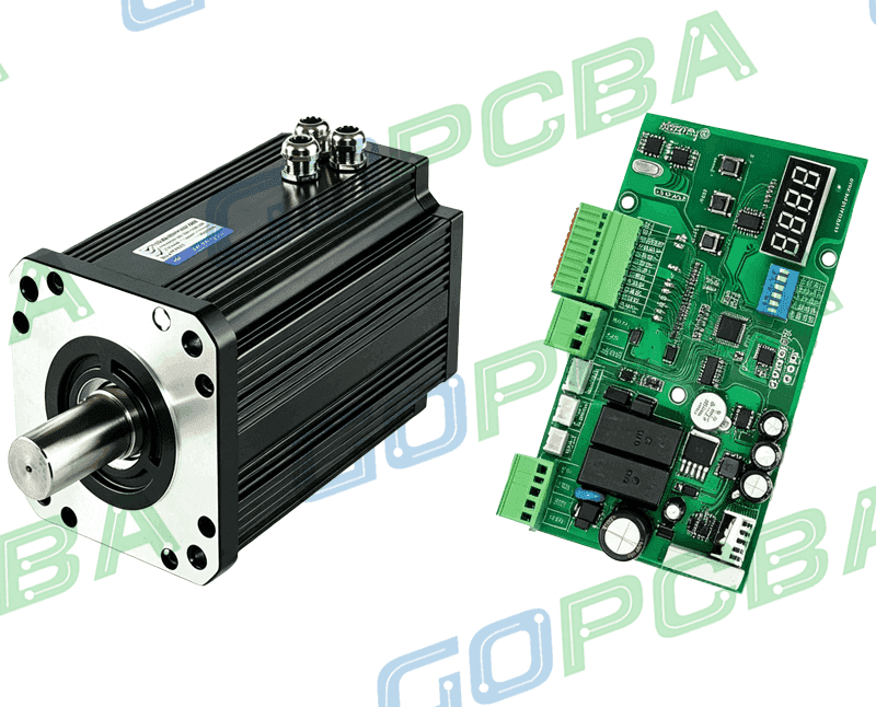
It helps to separate the two ideas. A coil board is defined by the shape of its conductors, while a module board is defined by function: a power module, a display module or a clock module is a board that can be plugged into a main board to avoid redesigning the same circuit twice.
The distinction matters commercially. A module board is reused across product variants, while a coil board is designed for one electrical function and its value is in the geometry rather than in the circuit around it.

Inductance and Geometry
Inductance grows with the square of the number of turns and with the area enclosed by them. Practical flat spirals reach a few microhenries in a footprint of a couple of square centimetres, which is enough for sensing coils and for small power converters.
Because the turns are close together on one layer, the winding capacitance is significant. It sets a self resonant frequency above which the part no longer behaves as an inductor, and that limit is usually what constrains the design.
Trace Width and Resistance
Direct current resistance follows the trace length, the copper thickness and the width. Widening the conductor reduces resistance but also reduces the number of turns that fit in the same area, so the two requirements have to be traded against each other.
For anything that carries alternating current, the conductor thickness that matters is the skin depth at the operating frequency rather than the full copper weight. Above a few megahertz, additional copper adds capacitance more than it adds conductance.
Quality Factor
The quality factor is the ratio of stored to dissipated energy, and it is limited by the winding resistance, the substrate loss and the radiation from the coil. A sensing coil with a low quality factor has a broad, shallow resonance that is difficult to read reliably.
Keeping the coil away from lossy material and using a substrate with a low loss tangent raises the figure. Where a magnetic material is used to increase the inductance, its loss at the operating frequency has to be considered as part of the same calculation.
Layer Stackup and Planes
A coil must not be placed over a solid copper plane. The image current induced in the plane cancels part of the field and destroys the inductance, so the layer directly beneath a sensing coil is normally left clear.
Where a ground reference is needed nearby it should be kept at a distance and slotted rather than solid. On a multilayer stack, the coil is usually placed on an outer layer with a wide keep out region beneath it.
Applications
Inductive position sensing, current measurement, wireless power transfer, near field communication antennas and rotary encoders are all built with printed windings. In each case the coil defines the field, and the circuit around it only conditions the signal.
The same geometry is used in reverse as a receiver. A pair of coupled printed coils forms a transformer with a defined turns ratio, which is convenient for isolated power in a low profile assembly.
Design Rules for Printed Windings
Keep the spacing between turns as uniform as the manufacturing tolerance allows, because a variation in spacing appears as a variation in the coupling and in the distributed capacitance. Round the corners of the spiral to reduce current crowding.
Bring the inner end of the winding out through a via on another layer, and treat the cross over as part of the design rather than an afterthought. The pad geometry at the terminals follows the same rules as any other conductor.
Thermal Behaviour
A coil carrying current heats up in its own resistance, and because the copper is thin the temperature rise can be larger than the circuit around it expects. Thermal vias under the winding help, but they also add capacitance to the coil.
Where the coil is used for wireless power, the accepted power has to be conducted away rather than radiated. A thermal path from the coil area to the enclosure is part of the design of the product.
Testing and Tolerance
Inductance is measured on a fixture that defines the test frequency and the fixture capacitance, because the reading depends on both. Comparing measurements taken on different instruments is the most common source of apparent tolerance failures.
Copper thickness tolerance, etch tolerance and substrate thickness tolerance all shift the inductance, so the specified tolerance should be realistic for the process rather than for the calculation.
Additional Considerations for This Build
Practical attention to spiral winding pays for itself here, because it decides whether the finished board behaves as the drawing intended. Where the requirement is not stated on the fabrication drawing or in the assembly notes, the shop has to assume a default, and that default is rarely the value the design was simulated with. Stating spiral winding explicitly, together with the tolerance that applies, removes the assumption and keeps the result predictable from batch to batch.
Process Control and Verification
On a design of this kind, inductance is the item that decides how the rest of the board is arranged. Keeping a sample from the panel turns a dispute into a measurement, because the same coupon can be re-examined by both parties without rebuilding the batch. Reviewing the design before the data is released is cheaper than correcting it after the panel is in the tank, because every step downstream inherits the decision made at the front end.
Documenting the assumption is part of the design work, and a short note on the drawing prevents a question that would otherwise arrive a day later and cost a day of schedule.
Related reading: our fabrication notes, board quality and design release notes cover the same ground.
FAQ
Why use a printed coil instead of a wound inductor? For repeatability, low profile and integration. Printed windings are defined by artwork, so every unit is identical, which matters for sensors and for arrays of coupled coils.
Can a coil be placed over a ground plane? Not without losing most of its inductance. The image current in the plane opposes the field, so the layer beneath the winding is left clear or heavily slotted.
How is the coil area connected to the rest of the circuit? The inner terminal is brought out through a via to another layer. The via and the cross over layer are part of the design and follow the usual pad and clearance rules.