In today’s fast-moving electronics industry, speed, precision, and reliability are essential for turning an innovative idea into a functional product. Engineers may spend weeks or months refining a circuit design, but until the design is physically manufactured, assembled, and tested, it remains only a digital blueprint.
The transition from a circuit design to functional hardware generally involves two closely connected stages: PCB fabrication and PCB assembly. While PCB fabrication creates the physical circuit board, prototype PCB assembly installs the electronic components and transforms the bare board into a functional PCBA that can be tested under real operating conditions.
For engineers, startups, and product developers, prototype PCB assembly is much more than simply soldering components onto a board. It is an important engineering validation stage that helps identify design, manufacturing, component, and functional issues before a product enters volume production.
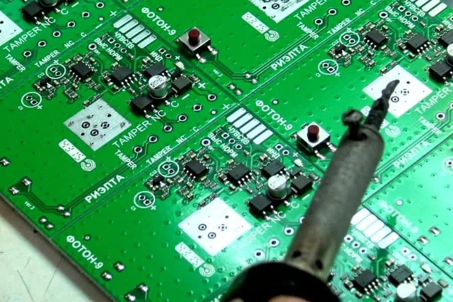
As an experienced PCB manufacturer and PCB assembly service provider, Kingda provides professional PCB prototype manufacturing, rapid PCB prototyping, and PCB assembly solutions, supporting customers from initial design verification through production. By integrating engineering review, PCB fabrication, component sourcing, assembly, inspection, and testing, Kingda helps streamline the transition from prototype development to reliable production.
What Are PCB Prototyping and Prototype Assembly?
Before discussing the manufacturing process, it is important to understand the difference between a PCB prototype and prototype PCB assembly. Although these two stages are closely related, they serve different purposes in the product development cycle.
1. PCB Board Prototype
A PCB board prototype is a physical, bare printed circuit board manufactured according to the customer’s PCB design files, typically including Gerber data, drill files, stack-up information, and other manufacturing specifications.
The main purpose of a PCB prototype is design validation. Instead of committing to a large production run immediately, engineers can manufacture a small quantity of boards to verify whether the circuit design can be manufactured and perform as expected.
A bare PCB typically contains:
- Copper traces for electrical signal and power transmission
- Pads for mounting electronic components
- Vias for connecting different PCB layers
- Solder mask for insulation and soldering protection
- Silkscreen for component references, labels, and markings
- Substrate materials such as FR-4, high-Tg materials, flexible materials, or specialized high-frequency laminates
A PCB prototype allows engineers to identify potential problems at an early stage, including incorrect footprints, insufficient spacing, routing problems, thermal concerns, impedance issues, and mechanical conflicts.
Early-stage design revisions are generally easier and less expensive than modifications made after mass production has started. Therefore, rapid PCB prototyping plays an important role in reducing development risk and accelerating product development.
2. Prototype PCB Assembly
Prototype PCB assembly is the process of mounting and soldering electronic components onto a bare PCB prototype to create a functional printed circuit board assembly (PCBA).
Unlike bare-board fabrication, prototype assembly brings the electrical design to life. Once components have been installed, engineers can power the board, load firmware, measure electrical signals, perform functional testing, and evaluate the product under realistic operating conditions.
A professional prototype PCB assembly service normally follows the customer’s Bill of Materials (BOM) and assembly drawings. Depending on the design, the process may include:
- Surface Mount Technology (SMT)
- Through-Hole Technology (THT)
- Solder paste printing
- Pick-and-place component placement
- Reflow soldering
- Wave or selective soldering
- Automated Optical Inspection (AOI)
- X-ray inspection
- Electrical testing
- Functional testing
For modern electronic products using miniature components and high-density packages, professional assembly equipment and process control are essential for achieving consistent soldering quality and placement accuracy.
Why Is Prototype PCB Assembly Important?
Prototype PCB assembly serves as the bridge between theoretical circuit design and real-world electronic performance.
A PCB design may appear correct during simulation but still encounter unexpected issues after physical assembly. For example, component tolerances, parasitic effects, thermal behavior, soldering conditions, mechanical interference, or PCB manufacturing limitations may affect actual performance.
A properly managed prototype assembly process helps answer several critical engineering questions.
Is the Design Manufacturable?
Prototype assembly verifies whether components can be placed and soldered correctly according to the design.
Engineers can identify problems such as:
- Insufficient component clearance
- Incorrect footprints
- Difficult-to-access solder joints
- Inadequate pad design
- Excessively dense component placement
- Conflicts between components and mechanical structures
Does the Circuit Work as Intended?
Once the prototype PCBA is assembled, engineers can perform electrical and functional tests to determine whether the circuit meets its design objectives.
This may include checking:
- Voltage and current
- Signal integrity
- Power consumption
- Communication interfaces
- Thermal performance
- Firmware operation
- Sensor performance
- Functional response under different operating conditions
Is the Design Ready for Mass Production?
Prototype assembly also provides valuable feedback for Design for Manufacturability (DFM) and Design for Assembly (DFA).
The lessons learned during prototype production can be used to optimize:
- Component selection
- PCB layout
- Pad and footprint design
- Component spacing
- Assembly sequence
- Testing methods
- Production yield
- Manufacturing cost
By identifying problems before volume production, companies can reduce engineering changes, minimize material waste, and improve the transition from prototype to mass production.
Professional Prototype PCB Assembly Process
A professional prototype PCB assembly process combines engineering review, automated manufacturing, inspection, and testing. Although the exact process varies according to board design and component requirements, a typical workflow includes the following stages.
Step 1: Engineering Review and DFM Analysis
Before assembly begins, the manufacturer reviews the PCB design files and BOM.
A professional DFM check evaluates whether the design can be manufactured and assembled efficiently. Engineers may review:
- PCB layer structure
- Component spacing
- Pad and footprint dimensions
- Solder mask clearance
- Via placement
- Assembly orientation
- Component availability
- Manufacturing tolerances
- Test-point accessibility
This early review helps identify potential production risks before materials are purchased or boards are assembled.
At Kingda, engineering support can be integrated into the prototype manufacturing process to help customers identify potential manufacturability and assembly issues before production.
Step 2: PCB Prototype Manufacturing
After the design is reviewed, the bare PCB is manufactured according to the approved specifications.
Depending on the application, the PCB may use materials such as:
- FR-4
- High-Tg FR-4
- Flexible PCB materials
- Rigid-flex materials
- High-frequency laminates
- Metal-core materials
The PCB manufacturing process may include imaging, copper pattern formation, lamination, drilling, plating, solder mask application, surface finishing, electrical testing, and final inspection.
The finished bare board then becomes the foundation for the prototype PCB assembly process.
Step 3: Solder Paste Printing
For SMT assembly, solder paste is applied to designated PCB pads through a precision stencil.
The solder paste contains solder alloy particles and flux. During reflow, the solder melts and forms the electrical and mechanical connection between the component terminals and PCB pads.
Printing accuracy is critical because excessive solder can cause bridges, while insufficient solder can result in weak or incomplete joints.
Modern solder paste printers use vision alignment systems and controlled printing parameters to improve consistency. Solder Paste Inspection (SPI) may also be used to measure paste volume, height, area, and position before component placement.
Step 4: Pick-and-Place Component Placement
After solder paste printing, SMT components are accurately positioned on the PCB using automated pick-and-place machines.
The machines retrieve components from reels, trays, or other feeders and place them onto the corresponding PCB pads according to the assembly program.
Modern SMT equipment can handle a wide range of components, from miniature passive devices to complex IC packages.
Depending on the project, prototype assembly may involve:
- 0201 and 0402 passive components
- QFP packages
- QFN packages
- BGA packages
- Connectors
- Sensors
- Microcontrollers
- Power management devices
For prototype and low-volume production, the assembly system must provide both flexibility and accuracy because product designs may change frequently during development.
Step 5: Reflow Soldering
After component placement, the populated PCB enters a reflow oven.
The board passes through controlled temperature zones that gradually heat the assembly, activate the flux, melt the solder, and then cool the solder joints.
A typical reflow profile consists of:
- Preheating – Gradually increases the PCB temperature and reduces thermal shock.
- Soaking – Stabilizes the temperature across the board and allows the flux to activate.
- Reflow – Raises the assembly above the solder alloy’s liquidus temperature so the solder forms reliable joints.
- Cooling – Controlled cooling solidifies the solder joints and completes the process.
The reflow profile must be optimized according to the PCB material, component package, solder alloy, board thickness, and thermal characteristics.
Poor thermal control can contribute to solder defects, component damage, warpage, or inconsistent solder joints.
Step 6: Through-Hole Component Assembly
Although SMT is widely used in modern electronics, some products still require Through-Hole Technology (THT).
THT components have leads that pass through drilled holes in the PCB. They are commonly used for:
- Connectors
- Large capacitors
- Transformers
- Power components
- Relays
- Components exposed to mechanical stress
Depending on the product and production volume, THT components can be inserted manually or automatically.
After insertion, they may be soldered using:
- Wave soldering
- Selective soldering
- Manual soldering
Selective soldering is particularly useful for mixed-technology boards where only specific through-hole areas require soldering while sensitive SMT components must be protected from unnecessary thermal exposure.
Step 7: Inspection and Quality Control
Inspection is a critical part of prototype PCB assembly because identifying defects early can prevent incorrect conclusions during design validation.
Common inspection technologies include:
AOI (Automated Optical Inspection)
AOI systems use cameras and image-processing algorithms to identify issues such as:
- Missing components
- Incorrect components
- Component misalignment
- Solder bridges
- Insufficient solder
- Polarity errors
- Other visible assembly defects
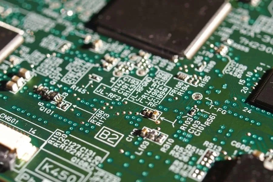
X-Ray Inspection
X-ray inspection is particularly useful for hidden solder joints that cannot be inspected optically. It is commonly applied to packages such as:
- BGA
- QFN
- LGA
- Other bottom-terminated or hidden-joint packages
X-ray inspection can help identify voids, opens, shorts, insufficient solder, and other hidden defects.
Step 8: Electrical and Functional Testing
After assembly and visual inspection, the prototype PCBA can undergo electrical and functional testing.
Common methods include:
In-Circuit Testing (ICT) checks individual circuits, components, and electrical connections where suitable test access is available.
Functional Circuit Testing (FCT) evaluates whether the completed PCBA performs according to its intended operating requirements.
Depending on the product, testing may include:
- Power-up testing
- Voltage and current measurement
- Signal testing
- Communication interface testing
- Firmware programming
- Sensor calibration
- Load testing
- Functional simulation
Testing is especially important during prototype development because the objective is not only to confirm assembly quality but also to validate the complete electronic design.
From PCB Prototype to Complete PCBA: Kingda’s Turnkey Solution
For engineers and product developers, coordinating separate suppliers for PCB fabrication, component sourcing, assembly, and testing can increase communication complexity and lead time.
A turnkey PCB assembly service integrates these processes under one manufacturing partner.
As an experienced PCB manufacturer and PCB assembly service provider, Kingda can support customers throughout the product development and manufacturing process, from prototype development to production.
Kingda’s Key Advantages
1. Integrated PCB Fabrication and Assembly
Kingda can support both PCB prototype manufacturing and PCB assembly, reducing the need to coordinate multiple suppliers for different manufacturing stages.
This integrated approach helps improve communication between PCB fabrication and assembly engineering teams.
2. Rapid PCB Prototyping
Prototype development often requires short lead times and fast engineering feedback. Kingda provides rapid PCB prototyping and prototype assembly solutions to help customers move quickly from design files to physical test boards.
3. Professional DFM Engineering Support
Before production, Kingda can review PCB design data and manufacturing requirements to identify potential DFM and assembly issues.
Early engineering feedback can help reduce design revisions, production risks, and unnecessary manufacturing costs.
4. SMT and THT Assembly Capability
Kingda supports different assembly technologies, including SMT assembly, THT assembly, and mixed-technology PCB assembly.
This flexibility enables the assembly process to be adapted to different component types and product requirements.
5. Component Sourcing Support
A complete PCBA project requires reliable component procurement as well as PCB manufacturing and assembly.
Kingda can support BOM-based component sourcing, helping customers coordinate components, PCB fabrication, and assembly within a streamlined production workflow.
6. Comprehensive Inspection and Testing
Quality control is integrated throughout the manufacturing process. Depending on project requirements, inspection and testing may include SPI, AOI, X-ray inspection, electrical testing, and functional testing.
These processes help identify assembly defects and verify that the completed PCBA meets the required specifications.
7. Support from Prototype to Production
A major advantage of working with an integrated PCB and PCBA manufacturer is the ability to maintain manufacturing continuity as the project develops.
After prototype validation, the same engineering and manufacturing workflow can be optimized for small-batch production and volume manufacturing, helping reduce unnecessary transition costs and shorten the path from development to commercialization.
Prototype Assembly vs. Mass Production Assembly
Prototype assembly and mass production share many fundamental technologies, but their manufacturing priorities are different.
| Feature | Prototype PCB Assembly | Mass Production PCB Assembly |
|---|---|---|
| Primary objective | Design validation | High-volume production |
| Production quantity | Low to small batch | Medium to high volume |
| Engineering changes | Frequent | Relatively limited |
| Manufacturing flexibility | Very important | Automation and throughput are critical |
| Component sourcing | Small quantities may be required | Stable long-term supply is important |
| DFM optimization | High priority | Essential for yield and cost control |
| Testing | Design and functional validation | Automated production testing |
| Production optimization | Fast iteration | High efficiency and repeatability |
A reliable manufacturing partner should therefore be able to support both prototype PCB assembly and subsequent production stages.
Common Prototype PCB Assembly Challenges
Prototype assembly is designed to identify problems early, but several challenges can still occur during manufacturing.
Component Availability
Prototype quantities are often small, while some components may have long lead times or limited availability.
Early BOM review and alternative component planning can help reduce delays.
Miniaturized Components
Small packages such as 0201, fine-pitch QFN, and BGA devices require accurate printing, placement, and soldering.
As component density increases, process control becomes increasingly important.
Soldering Defects
Typical defects include:
- Solder bridges
- Insufficient solder
- Excess solder
- Tombstoning
- Voids
- Cold solder joints
- Component misalignment
Proper stencil design, solder paste control, placement accuracy, and reflow profiling can significantly reduce these problems.
Design Changes
Prototype projects often involve multiple PCB revisions.
A flexible manufacturing process with clear revision control is therefore important for preventing outdated files or components from entering production.
Testing Complexity
Some prototype PCBAs require specialized test fixtures, programming, calibration, or functional simulation.
The manufacturer should understand the customer’s test requirements before assembly begins.
How to Choose a Reliable Prototype PCB Assembly Manufacturer
Choosing the right prototype PCB assembly manufacturer can have a significant impact on development speed, product quality, and eventual production costs.
When evaluating a supplier, consider the following factors:
Engineering Capability
The manufacturer should have experienced engineers who understand PCB fabrication, SMT, THT, DFM, DFA, and testing requirements.
Manufacturing Equipment
Check whether the supplier has suitable solder paste printers, SPI systems, pick-and-place machines, reflow ovens, AOI, X-ray equipment, and testing systems.
Component Sourcing
Reliable component procurement is essential for avoiding counterfeit parts, shortages, and unexpected production delays.
Quality Management
Look for documented quality processes and appropriate certifications for your target application and market.
Traceability
Production traceability allows manufacturers to track materials, processes, inspection results, and production batches. This is particularly important for products requiring strict quality management.
Prototype-to-Production Capability
A supplier that can support both prototype PCB assembly and volume PCB assembly can provide greater continuity as your product moves from engineering validation to commercialization.
Conclusion
Prototype PCB assembly is a critical stage between PCB design and finished electronic products. It transforms a bare PCB prototype into a functional PCBA that engineers can power, program, test, and evaluate under real operating conditions.
A professional prototype assembly process typically includes DFM review, PCB fabrication, solder paste printing, SMT component placement, reflow soldering, THT assembly, AOI, X-ray inspection, electrical testing, and functional testing.
More importantly, prototype assembly provides valuable engineering feedback before mass production. By identifying design and manufacturing problems early, companies can improve product reliability, optimize manufacturability, reduce production risks, and accelerate time-to-market.
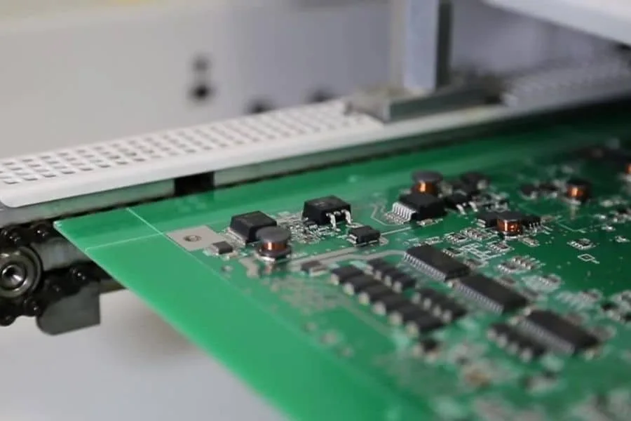
As an experienced PCB manufacturer and PCB assembly service provider, Kingda offers integrated PCB prototyping, rapid PCB manufacturing, component sourcing, SMT assembly, THT assembly, inspection, and testing solutions. From initial design verification to small-batch production and volume manufacturing, Kingda helps customers establish a streamlined path from PCB design to functional prototype and reliable production.