Satellite Communication High Frequency PCB: Design and Manufacturing Guide
Satellite communication systems are becoming increasingly important for navigation, remote sensing, broadband connectivity, defense-related communications, and other applications that require reliable data transmission over long distances. As operating frequencies and data rates continue to increase, the performance of the printed circuit board becomes an important factor in maintaining signal quality and system stability.
At the center of these electronic systems is the Satellite Communication High Frequency PCB, which provides the electrical platform for RF circuits, antennas, signal-processing devices, power-management circuits, and communication interfaces.
Unlike conventional FR-4 circuit boards used in many low-frequency applications, high-frequency PCBs for satellite communication require more careful consideration of dielectric properties, signal loss, impedance control, layer structure, material stability, thermal performance, and manufacturing tolerances.
A properly designed Satellite Communication PCB can help reduce transmission loss, maintain signal integrity, control electromagnetic interference, and provide a reliable foundation for high-frequency communication equipment.
What Is a Satellite Communication High Frequency PCB?
A Satellite Communication High Frequency PCB is a specialized printed circuit board designed for electronic systems operating at relatively high frequencies, including satellite communication equipment, RF modules, antenna systems, navigation equipment, radar-related electronics, and ground communication infrastructure.
The PCB may integrate:
- RF transmission circuits
- RF receiving circuits
- Antenna interfaces
- Power amplifiers
- Low-noise amplifiers
- Filters
- Mixers
- Frequency conversion circuits
- Signal-processing circuits
- Control circuits
- High-speed digital interfaces
- Power-management circuits
In these systems, the PCB is not simply a mechanical carrier for electronic components. Its dielectric characteristics, copper geometry, layer arrangement, surface finish, and routing structure can directly influence RF performance.
For this reason, PCB material selection and manufacturing should be considered together with the electrical design from the beginning of the project.
Why High-Frequency PCBs Are Important for Satellite Communication
Satellite communication systems must transmit and receive signals over long distances while maintaining sufficient signal quality.
Any unnecessary loss, impedance discontinuity, reflection, or electromagnetic interference can affect system performance.
A high-frequency PCB therefore needs to address several important factors.
Low Dielectric Loss
At higher frequencies, dielectric loss can become increasingly significant.
The laminate’s dielectric constant and dissipation factor influence how electromagnetic energy propagates through the PCB.
Low-loss materials can help reduce attenuation and support more efficient signal transmission, particularly in RF and microwave applications.
The appropriate material should be selected according to:
- Operating frequency
- Required insertion loss
- Dielectric constant
- Dissipation factor
- Thermal environment
- Mechanical requirements
- Manufacturing process
- Cost objectives
Controlled Impedance
Impedance control is one of the most important requirements for many high-frequency PCB designs.
Transmission lines need to maintain a predictable impedance throughout the signal path. Variations in trace width, copper thickness, dielectric thickness, or layer registration can change the actual impedance.
Controlled-impedance design therefore requires coordination between PCB layout and manufacturing.
Critical parameters can include:
- Trace width
- Trace thickness
- Dielectric thickness
- Copper roughness
- Reference-plane distance
- Layer structure
- Via geometry
- Connector design
For complex RF and high-speed designs, professional PCB Design and Layout can help engineers develop an appropriate stackup and routing strategy before fabrication.
High-Frequency PCB Materials for Satellite Applications
Material selection has a direct influence on high-frequency electrical performance.
Conventional FR-4 materials can be suitable for many digital and lower-frequency circuits, but specialized high-frequency laminates may be preferred when low dielectric loss and stable electrical characteristics are required.
PTFE-Based Materials
PTFE-based laminates are commonly considered for demanding RF and microwave applications because of their low dielectric loss.
They can be useful in antenna circuits, RF front ends, filters, and other applications where signal attenuation must be carefully controlled.
However, PTFE-based materials may require specialized manufacturing processes because their mechanical and dimensional characteristics differ from conventional FR-4 materials.
High-Frequency Hydrocarbon-Ceramic Materials
Hydrocarbon-ceramic laminates can provide a combination of relatively low loss, controlled dielectric properties, and manufacturing characteristics suitable for certain RF applications.
These materials may be used where engineers need to balance electrical performance, mechanical stability, and production requirements.
Hybrid Material Construction
Some satellite communication boards combine different PCB materials within a single multilayer structure.
For example, a design may use a high-frequency laminate for RF layers while using FR-4 for selected digital or control layers.
This hybrid construction can help balance electrical performance and manufacturing cost.
However, mixed-material stackups require careful control of:
- Thermal expansion
- Lamination parameters
- Layer registration
- Resin compatibility
- Dielectric thickness
- Copper bonding
- Mechanical stress
Multilayer Construction for Satellite Communication PCBs
Modern satellite communication equipment often integrates RF, high-speed digital, control, and power functions into compact assemblies.
A multilayer PCB can provide the required routing density while allowing different electrical functions to be separated across dedicated layers.
A typical stackup may include:
- RF signal layers
- High-speed digital layers
- Ground planes
- Power planes
- Control signal layers
A carefully designed multilayer structure can improve:
- Signal integrity
- Power integrity
- EMI performance
- Routing density
- Thermal distribution
- Mechanical stability
Ground planes are particularly important because they provide controlled return paths for high-frequency signals.
The relationship between signal traces and reference planes should therefore be considered during stackup development rather than only after routing has been completed.
RF Signal Integrity and Loss Control
The primary objective of a High-Frequency PCB is to maintain predictable signal behavior throughout the transmission path.
At high frequencies, relatively small variations in PCB geometry can influence electrical performance.
Trace Geometry
RF transmission lines should be designed according to the target impedance and selected PCB material.
Important parameters include:
- Trace width
- Copper thickness
- Dielectric thickness
- Trace-to-ground spacing
- Copper surface characteristics
- Transmission-line geometry
The final manufactured dimensions should remain within appropriate process tolerances.
Via Transitions
Vias can introduce discontinuities into high-frequency signal paths.
When an RF signal transitions between PCB layers, the via structure should be designed to minimize unwanted parasitic effects.
Depending on the frequency and circuit architecture, engineers may consider:
- Via diameter
- Pad size
- Antipad dimensions
- Via stub length
- Ground-via placement
- Signal-via configuration
Blind vias and other advanced interconnection technologies can sometimes reduce unnecessary via stubs and improve routing flexibility.
EMI and Electromagnetic Compatibility
Satellite communication equipment often operates alongside multiple RF, digital, and power circuits.
Electromagnetic interference can therefore become an important design challenge.
A robust Satellite Communication PCB design may incorporate:
- Continuous ground planes
- Controlled return-current paths
- RF shielding
- Filtering
- Physical separation of functional blocks
- Proper connector placement
- Optimized power distribution
- Short high-frequency signal paths
Sensitive RF circuits should be separated from noisy switching regulators and high-current digital circuits wherever practical.
The enclosure and PCB should also be considered together because shielding effectiveness depends on the complete system architecture.
Thermal Management in High-Frequency PCB Design
Although signal integrity is a primary concern, thermal performance should not be overlooked.
Satellite communication equipment can contain components such as:
- Power amplifiers
- RF transistors
- Voltage regulators
- Processing devices
- High-power transmit circuits
These components can generate localized heat.
A suitable PCB thermal design may use:
- Large copper areas
- Thermal vias
- Copper planes
- Heat-spreading structures
- Thermal interfaces
- Appropriate component placement
- External heatsinks where required
Thermal design should consider both the PCB and the complete mechanical enclosure.
For applications involving significant power dissipation, engineers should evaluate temperature distribution during the design stage rather than relying only on physical testing after production.
Precision PCB Manufacturing Requirements
The electrical performance of a Satellite Communication High Frequency PCB depends heavily on manufacturing consistency.
Small variations in layer registration, dielectric thickness, copper geometry, or surface finish can affect high-frequency performance.
Layer Registration
Multilayer RF boards require accurate alignment between signal layers and their corresponding reference planes.
Poor registration can change transmission-line geometry and affect impedance.
Manufacturing processes should therefore control:
- Lamination movement
- Layer alignment
- Drill registration
- Imaging accuracy
- Copper pattern dimensions
Copper Thickness and Surface Characteristics
Copper thickness influences both electrical resistance and transmission-line geometry.
For high-frequency applications, conductor surface characteristics can also influence signal loss because of skin-effect behavior.
The appropriate copper structure should therefore be selected according to the electrical requirements and manufacturing capabilities.
Precision Drilling
Drilling accuracy becomes particularly important when the PCB contains dense RF routing, small vias, blind vias, or buried vias.
Manufacturing control should address:
- Hole diameter
- Hole position
- Drill-to-pad registration
- Hole-wall quality
- Plating consistency
- Via structure
A controlled PCB Manufacturing process helps connect the electrical requirements defined during design with the dimensional consistency required during fabrication.
Surface Finish Selection
The PCB surface finish affects solderability, pad quality, oxidation resistance, and assembly performance.
For fine-pitch and RF components, a relatively flat surface can be important for reliable assembly.
Potential surface finishes include:
- ENIG
- ENEPIG
- OSP
- Immersion tin
- HASL
The appropriate finish depends on the component package, assembly process, storage requirements, environmental conditions, and product specifications.
For high-frequency applications, the effect of surface characteristics on RF performance should also be considered where applicable.
Fine-Line and High-Density PCB Technology
Satellite communication systems increasingly require smaller equipment with greater functionality.
This creates demand for compact high-density PCB structures.
Advanced manufacturing technologies may include:
- Fine-line routing
- Microvias
- Blind vias
- Buried vias
- High-layer-count multilayer boards
- HDI structures
- Sequential lamination
These technologies allow engineers to place more functionality into limited PCB space.
However, higher-density construction also increases manufacturing complexity. PCB manufacturers must maintain tighter control over imaging, drilling, plating, lamination, and layer registration.
PCB Assembly for Satellite Communication Electronics
Bare-board fabrication is only one part of the manufacturing process.
The completed PCB Assembly must also provide reliable electrical and mechanical performance.
Satellite communication boards may include RF components, processors, power devices, connectors, filters, oscillators, memory devices, and fine-pitch packages.
A controlled assembly process can include:
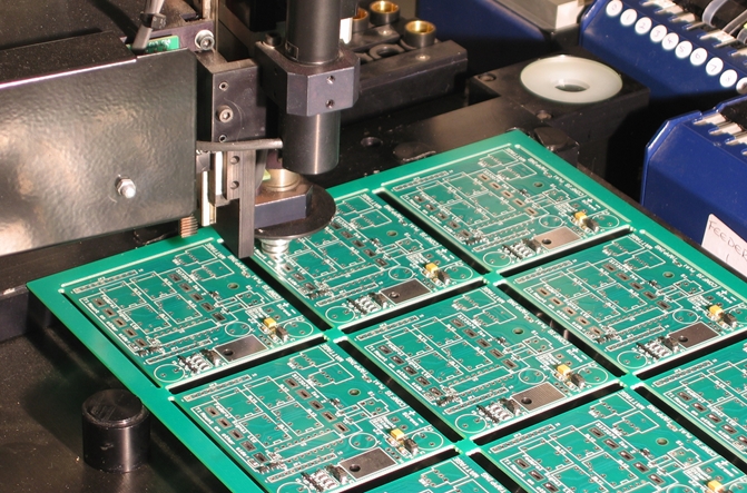
- Solder-paste printing
- Solder-paste inspection
- SMT placement
- Reflow soldering
- Automated optical inspection
- X-ray inspection where appropriate
- Through-hole assembly
- Electrical testing
- Functional testing
Component placement is particularly important for RF circuits because the physical relationship between components and transmission lines can influence circuit performance.
For new designs, Prototype PCB Assembly provides an opportunity to validate component placement, assembly quality, electrical performance, and mechanical compatibility before production quantities increase.
Quality Inspection and Testing
High-frequency PCB quality cannot be evaluated solely through visual inspection.
A comprehensive quality process may include multiple inspection methods.
Visual and Dimensional Inspection
Visual inspection can identify:
- Solder-mask defects
- Copper-pattern damage
- Scratches
- Contamination
- Board-edge defects
- Surface-finish problems
Dimensional inspection can verify board thickness, outline dimensions, hole positions, and other mechanical characteristics.
Electrical Testing
Electrical testing can verify:
- Continuity
- Isolation
- Short circuits
- Net connectivity
- Basic electrical characteristics
For controlled-impedance boards, additional impedance testing may be performed according to the project requirements.
Cross-Section Analysis
Cross-section analysis can be useful for evaluating multilayer construction and manufacturing quality.
It can provide information about:
- Copper thickness
- Plated-hole quality
- Dielectric thickness
- Layer registration
- Via construction
- Lamination quality
This can be particularly useful for complex high-frequency and multilayer PCB designs.
Reliability Considerations for Satellite Communication Electronics
Satellite communication equipment may need to operate reliably over long periods with limited opportunities for physical maintenance.
Depending on the application and system architecture, PCB reliability considerations may include:
- Thermal cycling
- Temperature exposure
- Humidity resistance
- Vibration
- Mechanical shock
- Electrical stress
- Insulation resistance
- Plating reliability
- Solder-joint reliability
For spaceborne applications, the requirements can be substantially different from those for terrestrial satellite communication infrastructure. Material selection, outgassing, radiation environment, thermal-vacuum conditions, and applicable aerospace requirements may need to be addressed separately.
Therefore, the PCB specification should always be developed according to the actual installation environment and system-level requirements.
Prototype Development and Design Validation
High-frequency communication systems often require multiple engineering iterations before the final design is released.
A typical development process can include:
- Define RF performance requirements
- Select PCB materials
- Develop the stackup
- Design controlled-impedance structures
- Complete RF and digital routing
- Perform DFM review
- Manufacture prototype PCBs
- Assemble components
- Conduct electrical testing
- Evaluate RF performance
- Validate thermal behavior
- Perform environmental testing where required
- Optimize the design
- Release the production version
Prototype validation can help identify problems such as excessive insertion loss, impedance deviations, thermal concentration, EMI issues, or mechanical interference before the design enters larger-scale production.
Components Procurement and Supply Chain Planning
Satellite communication electronics may contain specialized RF devices and components with limited availability.
Supply-chain planning should therefore begin during the engineering stage.
Engineers and purchasing teams may need to evaluate:
- Component lifecycle
- Availability
- Lead time
- Approved alternatives
- Package compatibility
- Electrical equivalence
- Manufacturer qualification
- Traceability
Coordinating PCB fabrication, assembly, and component sourcing can simplify the transition from prototype to production.
For projects requiring integrated sourcing support, Components Procurement can help align component availability with the PCB assembly schedule.
Designing High-Frequency PCBs for Manufacturability
A high-frequency PCB should not be designed solely for electrical performance.
Manufacturability needs to be considered from the beginning because extremely tight design requirements can increase production difficulty and cost.
Important DFM considerations include:
- Minimum trace width and spacing
- Controlled impedance tolerance
- Layer registration
- Drill diameter
- Via structure
- Copper thickness
- Surface finish
- Material availability
- Panelization
- Component spacing
- Test-point accessibility
Close communication between the PCB designer and manufacturer can help identify potential production risks before fabrication.
This is especially important for hybrid-material PCBs and advanced multilayer structures.
Future Development of Satellite Communication PCBs
The continued development of satellite communication technology is driving higher data rates, broader frequency ranges, smaller equipment, and greater integration.
Future Satellite Communication High Frequency PCB designs may increasingly require:
- Lower transmission loss
- Higher-frequency operation
- More compact layouts
- Advanced low-loss materials
- Higher layer counts
- Improved thermal management
- Greater RF and digital integration
- More precise impedance control
- Advanced HDI structures
As communication systems become more sophisticated, PCB engineering will increasingly need to combine RF design, mechanical engineering, thermal analysis, and manufacturing expertise.
Why High-Frequency PCB Quality Matters
The PCB is an important part of the signal path in satellite communication equipment.
A small manufacturing deviation can potentially affect impedance, signal loss, phase behavior, thermal performance, or electromagnetic compatibility.
A reliable Satellite Communication PCB should therefore combine:
- Appropriate low-loss materials
- Controlled impedance
- Stable multilayer construction
- Accurate layer registration
- Reliable copper plating
- Optimized RF routing
- Effective EMI control
- Thermal management
- Precision PCB Manufacturing
- Reliable PCB Assembly
- Comprehensive inspection and testing
The goal is not simply to produce a functional circuit board, but to maintain predictable electrical performance throughout the intended operating environment.
Conclusion
The Satellite Communication High Frequency PCB is a critical hardware foundation for modern satellite communication and RF electronics. It supports signal transmission, reception, processing, power management, and communication interfaces while helping engineers achieve the required electrical and mechanical performance.
Because high-frequency signals are sensitive to material properties, impedance variation, transmission-line geometry, layer registration, and electromagnetic interference, PCB development requires close coordination between design and manufacturing.
By selecting appropriate high-frequency materials, optimizing multilayer stackups, controlling impedance, minimizing signal loss, managing thermal performance, and applying reliable PCB Assembly processes, manufacturers can develop circuit boards suited to demanding satellite communication applications.
As satellite networks continue to evolve toward higher bandwidth, lower latency, broader coverage, and greater system integration, the importance of advanced High-Frequency PCB technology will continue to increase. Careful PCB engineering and manufacturing will remain essential for achieving stable and predictable performance in next-generation satellite communication systems.