Security Camera Main Board PCBA Assembly
A camera main board has to handle three things at once: the image, the network and the power. It carries a processor, memory, the network interface, the power conversion, the image sensor interface and the control circuit for the infra-red illumination, and the assembly has to satisfy more than an appearance check. If the image interface is rotated, if a network device is the wrong type or if the power section has a joint problem, the board can power up and still produce no picture or fail to establish a connection.
What the Order Needs
The Gerber data, the bill of materials, the coordinates, the assembly drawing, the quantity and the delivery date are the base documents. The bill of materials names the processor, the memory, the network device, the power components, the crystal and the connectors by full part number, and the assembly drawing marks the image interface, the ribbon connector and the orientation of every polarised part.
Where programming is included, the programme file, the target device, the programming interface and the method of reading the revision back are supplied. Many camera boards also have to carry individual data such as a network address or a serial number, and the rule for generating it, the position at which it is written and the check for a duplicate belong with the order rather than with the operator.
The functional test documentation states the supply conditions, the sensor module, the network connection, the image output and the procedure for the illumination interface. The test station and the connection scheme are assessed from the customer’s criterion rather than from an assumption about what the product is supposed to accept.
Assembling the Image Interface and the Fine Pitch Devices
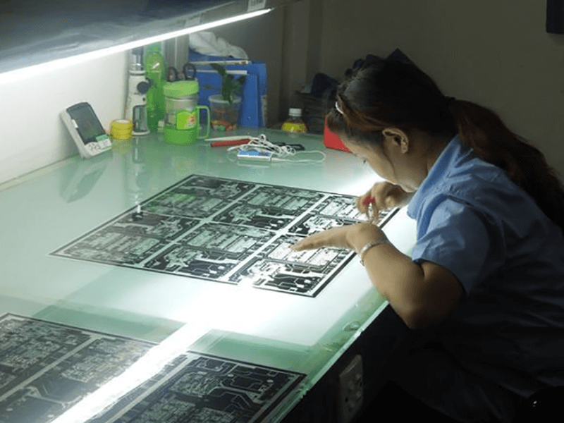
Before the order starts, the reference designators, the placement angles and the packages are checked against the bill of materials. The image sensor connector, the processor, the memory and the crystal are the parts where an orientation error or a coordinate deviation matters most.
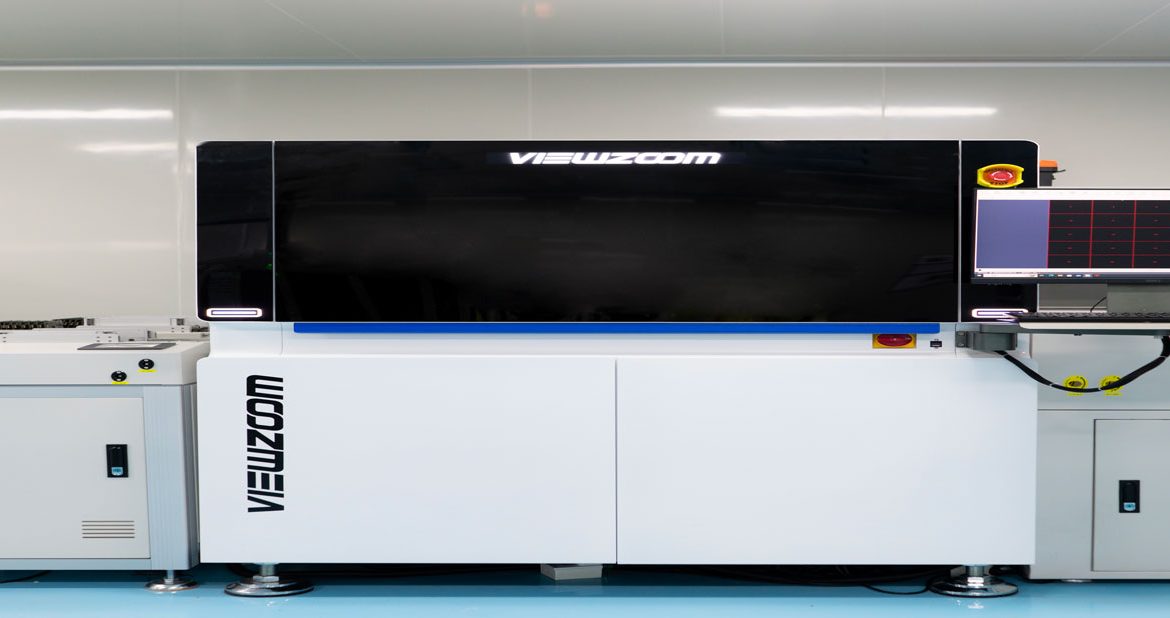
The stencil is evaluated in parts rather than as one pattern: the fine pitch leads, the heat spreading pad and the ordinary passives each need their own opening. After printing, SPI measures the area, volume and offset of the deposit so that a short or an excess is caught before the board reaches the placement machine.
The image sensor connector is sensitive to flatness and position. After the first article is placed, the connector is checked for offset and tilt, because a connector that is very slightly rotated can still be soldered correctly and still fail to seat a ribbon cable, which is a fault that only appears when the product is assembled.
Confirming the First Article After Reflow
After reflow, optical inspection covers the missing parts, the offset, the reversed parts and the visible joint anomalies, and an alarm from the machine is reviewed against the physical board rather than being judged from the reflection or the colour of the component body.
The first article also confirms the part numbers of the image interface, the network connector, the power devices and the memory. Where the order includes programming and test, the write, the read back of the revision and the basic functional verification the customer specified are completed as part of the same release.
When there is no video output, the investigation separates the programme, the sensor connection, the supply, the crystal and the soldering. When the network will not connect, the interface devices, the transformer, the programme and the test cable are examined together, because touching up the joints of the network connector is a repair carried out before the cause has been established.
Keeping the Addresses and the Revisions Apart
Once the board is in volume, the hardware revision, the programme revision and the individual identifier have to stay in correspondence. Boards that have not been programmed, boards that have been programmed successfully, boards that have passed the test and boards under repair are kept in separate flows, because a board that has been programmed with one revision and mixed into a group of another cannot be identified later.
When the customer updates the programme or the material, the batch from which the change applies is stated. Boards that are already programmed are not stored with the new revision, and a repaired board repeats the corresponding test rather than being released on the basis that it was working before.
Packing protects the parts most likely to be damaged: the sensor interface, the antenna connector and the ribbon connector, which stand proud of the board and are the first things to suffer in transit. Our SMT assembly lines place and inspect the board, PCBA testing covers the programming and the functional check, and the records are held under quality management.
Writing the Identifiers and Keeping the Records
Many camera boards leave the line with individual data written into them: a serial number, a product key, a calibration constant or a network address. The rule for generating that value, the interface it is written through and the way a duplicate is detected are defined by the customer and held with the order, because the identifier is not a production detail that the line can invent on its own.
Where a MAC address is written, the same discipline applies as for any other unique value. The block of addresses, the first and last value in the block, the device that performs the write and the position in the flow at which it happens are all stated, and the value is read back afterwards and checked against the record. Two boards carrying the same MAC address both pass on a bench and then conflict on a live network, which is a fault that surfaces at the customer’s site rather than on the assembly line.
The record for the batch follows the same principle. The material lot, the stencil revision, the placement programme, the reflow profile, the programming revision and the test result are held against the order, so a question about one particular board is answered from the documentation instead of from an inspection of the board itself.
Handling and packing complete the flow. The sensor interface, the antenna connector and the ribbon connector are the parts that stand proud of the board, and they are the parts that suffer first when the packing is inadequate or when boards are stacked without separation. Boards are held by the edges, and the finished goods travel in antistatic material with the protruding parts protected from compression.
A new camera design is best introduced through a small batch that confirms the Gerber data, the bill of materials, the coordinates, the identifier rule and the test flow in one pass. That batch becomes the reference for the volume orders, and customers who want the review extended to the artwork can raise it through PCB design and layout and the IoT PCBA route before the volume order is placed.
FAQ
Why does a board power up and show no image? Because the image path involves the programme, the sensor connection, the supply and the crystal as well as the joints, and the fault is in one of them rather than necessarily in the connector.
Who defines the network address rule? The customer, since the address has to be unique within the customer’s own network and must not be duplicated across boards.
What is checked on the first article? The paste condition, the placement, the orientation, the joints, the tilt of the image connector and the part numbers of the critical devices.