Single Layer PCB Manufacturing Guide: Process, Methods and Cost
Even as electronics move toward smaller, faster, and more complex designs, single layer PCB manufacturing remains the workhorse of the global electronics industry. Consumer devices, LED lighting drivers, power control boards, and industrial control modules all depend on single-sided boards because they combine low cost with dependable performance. If you are sourcing boards for a new product, understanding how a single layer PCB is fabricated helps you design for manufacturability, choose the right materials and finishes, and keep project costs under control. This single layer PCB guide explains the manufacturing process step by step, compares common fabrication methods, and gives practical advice on selecting a reliable PCB manufacturing partner.
What Is a Single Layer PCB?
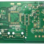
A single layer PCB, also called a single-sided PCB, is a circuit board with copper traces on only one side of the insulating substrate. The structure is simple: a base laminate, one patterned copper layer, a solder mask, and silkscreen markings. Because there is only one conductive layer, the board is inexpensive to build, easy to route, and fast to produce. That makes it the most widely used board type in the industry and a natural fit for low- and mid-complexity applications where dense interconnection is not required.
Compared with multilayer boards, single-sided designs involve fewer process steps and less material, which translates directly into lower unit cost and shorter lead times. The trade-off is limited routing space, so designers must plan trace paths carefully. For applications such as power adapters, remote controls, and LED drivers, the simplicity of a single layer PCB is a feature, not a limitation.
Core Materials for Single Layer PCB Manufacturing
Material choice affects both cost and performance of a single layer PCB. FR-4 fiberglass laminate is the most common substrate because it offers a good balance of mechanical strength, electrical insulation, and price for most electronic products. Aluminum-base boards are preferred for LED applications because the metal core conducts heat away from high-brightness emitters. Copper-base substrates are used in high-power, high-heat-load scenarios where thermal management is the dominant concern.
Standard board thickness ranges from 0.8 to 2.0 mm, and custom thicknesses are available for special enclosures. Copper weight is normally selected from 1 oz (35 microns) to 2 oz (70 microns), with heavier copper reserved for high-current circuits. When the specification is clear, a manufacturer can recommend the most economical substrate for the application, which is exactly why working directly with a fabrication partner early in the design cycle saves money.
Complete Single Layer PCB Manufacturing Process
The typical production flow for a single-sided board moves through a series of well-defined steps. First, the base laminate is cut to panel size from raw sheets. The copper surface is then cleaned and roughened to improve adhesion of the photoresist. A photosensitive dry film or liquid resist is coated onto the copper, followed by UV exposure through the pattern and development of the image. Chemical etching removes the unwanted copper, leaving only the designed traces. After stripping the resist, the board is drilled, coated with solder mask, and finished with silkscreen printing. Surface finishing, electrical testing, and final packaging complete the process.
Every step affects conductivity and service life. Inconsistent etching can produce weak traces, poor solder mask adhesion can expose copper to oxidation, and inaccurate drilling can shift mounting holes. A factory with disciplined process controls and PCB capabilities that match your design will catch these issues before they reach the assembly line.
Common Manufacturing Methods Explained
Several methods are used to form the copper pattern on a single layer PCB. Subtractive etching is the mainstream approach: chemical solution removes copper from non-circuit areas, producing uniform traces at high volume and low cost. CNC milling cuts the copper layer with mechanical tools, which suits prototypes, small batches, and urgent deliveries because no photo tooling is required. Laser direct imaging exposes fine-pitch patterns without film, offering high accuracy for detailed designs. Screen-printed mask imaging is the traditional method and remains efficient for highly repetitive, large-volume orders.
Each method influences precision, delivery time, and total cost. A project in the concept stage may start with CNC-routed samples, then switch to subtractive etching for mass production. Understanding these options lets buyers plan a low-cost single layer PCB strategy that keeps quality consistent from prototype to volume.
Surface Finishing Options
Surface finish determines solderability and oxidation resistance. HASL hot air solder leveling is the lowest-cost option and works well with through-hole components, although surface flatness is limited. ENIG immersion gold provides excellent solderability and corrosion resistance, making it the recommended choice for fine-pitch SMT assembly. OSP organic solderability preservative is an environmentally friendly treatment suited to medium and large batches with short storage periods. Immersion silver offers outstanding conductivity but requires controlled storage conditions.
For most single layer boards, the finish should be selected according to assembly method and storage plan. A board that will be assembled quickly in high volume can use OSP, while boards that may sit in inventory or use fine-pitch parts benefit from ENIG. Matching the finish to the real production environment is a simple way to improve first-pass yield.
Drilling and Hole Formation
Single layer boards rarely use plated through-holes, but mechanical or laser drilling is still needed for connector mounting holes, LED heat-relief apertures, and metal support holes. Hole position tolerance is generally around plus or minus 0.05 to 0.1 mm. Misaligned holes affect assembly accuracy, so panel tooling and drill registration are checked carefully during fabrication. Even in a simple one-layer product, hole quality can determine whether a connector seats properly on the assembly line.

Copper Trace Design and Routing
Copper traces are the signal channels of the board, and their design deserves attention even on a single-sided layout. Minimum trace width and spacing define how much circuitry fits on the panel. Current-carrying capacity determines whether traces overheat under load. Thermal design keeps hot components from warping the board, and thermal pad treatment around vias improves solderability.
For high-current applications such as LED drivers, thicker copper of 35 to 70 microns is recommended to avoid heat buildup. Since only one side is available for routing, signal planning and component placement must be coordinated. A structured PCB design and layout review will confirm that trace widths, clearances, and pad sizes are manufacturable before tooling begins.
Solder Mask and Silkscreen
The solder mask protects the copper surface and serves several practical functions. It prevents solder bridges between adjacent pads, improves moisture resistance, stops copper oxidation, and improves the visual quality of the finished board. Single layer PCBs are available with green, black, blue, red, and white solder mask, and white is frequently chosen for LED lighting because it reflects light from the emitters.
Silkscreen printing marks component designators, polarity directions, and maintenance labels. Clear markings raise assembly efficiency, reduce maintenance cost, and speed up fault location. Layout guidelines keep silkscreen text away from pads and vias so the markings are never covered by solder or components.
Quality Inspection and Testing
Rigorous testing protects the reliability of every single layer PCB. AOI automatic optical inspection identifies shorts and opens by comparing the board image with the design database. Flying probe testing verifies electrical continuity without requiring a dedicated test fixture, which makes it efficient for prototypes and small batches. Continuity and resistance checks confirm that every net is correctly connected.
Testing is most valuable when it is matched to the product. A simple control board may only need AOI plus a basic continuity test, while a safety-related power board deserves more thorough electrical verification. Factories that follow documented quality systems, such as ISO 9001 and IPC standards, provide consistent results from batch to batch.
Typical Applications of Single Layer PCBs
Single layer boards are found in countless everyday products. LED lighting driver circuits, automotive signal lamps, simple power supply modules, temperature control boards, and remote control panels all rely on single-sided construction. The combination of simple structure, low cost, and proven reliability makes them the default choice whenever the circuit is not too complex.

Cost Factors for Single Layer PCBs
Price depends mainly on material grade, copper thickness, surface finish, hole count, and order volume. Because the process is short, unit pricing stays low even for small quantities. As a typical reference, prototype quantities run from USD 0.30 to USD 2.50 per piece, while volume production falls to USD 0.15 to USD 1.60 per piece. ENIG finish and heavy copper versions cost slightly more, reflecting the extra material and process time.
Requesting quotes with clear specifications is the fastest route to a realistic budget. When the same supplier handles low volume PCB assembly, the bare board and populated board can be coordinated in one program, which simplifies logistics and protects delivery dates.
Common Challenges in Single Layer PCB Manufacturing
Even simple boards have failure modes worth understanding. Copper traces can overheat when trace width is too small for the current. Solder mask misregistration may expose pads or leave mask over component footprints. Thermal warpage appears when panel design ignores heat distribution, and solder bridging occurs when pad spacing is too tight for the assembly process. Most of these risks are addressed during design review, before any copper is etched.
How to Choose a Reliable Single Layer PCB Manufacturer
Supplier selection should focus on certification, engineering support, and delivery stability. Look for UL and ISO certified facilities with DFM analysis capability, because a design-for-manufacturability review performed before production catches issues that cause delays later. Responsive engineering communication matters for custom materials, finishes, and special tolerances.
gopcb provides quick delivery of 3 to 7 working days, low minimum orders starting from 5 to 10 boards, and cost-effective processing for overseas volume customers. With experience across FR-4, aluminum-base, and copper-base single layer boards, gopcb supports projects from sample validation through mass production under one roof. Quality systems and process discipline at the factory follow ISO and IPC aligned practices.
Future Trends in Single Layer PCB Manufacturing
Single-sided board production is also evolving. AI-based visual inspection is improving defect detection, green and recyclable substrate materials are entering the market, automated routing optimization is shortening engineering time, and low-temperature solder mask technology is reducing energy use. These developments will make single layer PCB manufacturing more efficient and more reliable while keeping the cost advantage that makes these boards so popular.
Single Layer PCB Manufacturing FAQ
Q1: What is the standard lead time? Generally 3 to 7 working days depending on the surface finish and quantity.
Q2: What is the minimum trace width and spacing? Standard capability is 4/4 mil, with 3/3 mil available for advanced designs.
Q3: Can single layer boards be used for SMT assembly? Yes, and ENIG finish is recommended for better soldering flatness.
Q4: What is the minimum order quantity? Most orders can start from 5 to 10 pieces for prototypes.
Q5: What is the typical price of a single layer PCB? Prototypes are roughly USD 0.30 to USD 2.50 per piece and volume pricing runs from USD 0.15 to USD 1.60 per piece.
Conclusion
Single layer PCB manufacturing remains essential to the electronics industry because it delivers the lowest-cost, most reliable boards for a huge range of products. Choosing the right substrate, surface finish, and trace strategy improves reliability, while working with an experienced manufacturer keeps research, sampling, and mass production efficient and controllable. Whether you need a quick prototype or a large production order, a clear specification and the right quality management partner make the entire process predictable.