Single-Sided PCB Manufacturing: A Complete Guide
A single-sided board carries its copper pattern on one face only, which sounds like a limitation and is in fact the reason it survives. It is the cheapest board that can be fabricated, the fastest to turn around and the easiest to inspect, and for a large class of products that combination beats the density advantage of a multilayer stack. Lighting modules, power control boards, small appliances and countless educational and hobby designs are built this way, and the manufacturing sequence behind them is worth understanding because it explains the cost and the design rules.
What Single-Sided Construction Means
The laminate carries copper on one face. Components are mounted on that same face, and connections between them are made by the copper pattern rather than by vias. There are no plated through holes in the conventional sense, so the two faces of the board cannot be connected to each other at all unless a wire link or a crimped eyelet is added deliberately.
That single restriction is what defines the family. A double-sided board adds copper on the second face and plated holes to join the two, which immediately allows traces to cross under each other. A multilayer board extends the same idea to several layers with alternating dielectric and copper, and it is the only way to support controlled impedance, dense routing and a solid reference plane beneath high-speed signals. A single-sided board cannot do those things, but it also does not need lamination cycles, plating lines or layer registration, and those are the processes that dominate the cost and the lead time of everything else.
Substrate Choices and What They Cost
FR-4 is the default: a woven glass fabric bonded with a flame-retardant epoxy, stiff, dimensionally stable and available in every thickness and copper weight. Where cost pressure is extreme, phenolic paper laminate is used instead, because it is cheaper and punches and shears more easily, at the price of poorer mechanical strength, worse moisture resistance and a lower temperature rating. Aluminium-backed laminate appears where the circuit generates heat, since the metal core spreads it laterally far better than any glass-reinforced plastic, but it can only be used where the copper pattern is simple enough that the single conductive face is sufficient.
Copper weight matters as much as the base material. One ounce per square foot is the usual starting point, and it is adequate for signal routing and for modest currents. Where the board carries motor or lamp current, two ounces or more reduce the voltage drop and the self-heating, and they also make the etching process less critical because a thicker foil resists undercut better. Thinner copper foil down to half an ounce is used where fine lines are needed on a low-current board, but the gain in resolution is usually small and the fragility of the traces grows quickly.
From Copper Clad Laminate to Finished Board
Fabrication starts with a sheet of copper clad laminate cut to panel size. Holes are drilled, or punched where the volume justifies a die, and the drilling data comes directly from the layout file. Because there is no plating step, the hole is simply a mechanical clearance for a component lead, and the electrical connection is made by the solder fillet on the copper side.
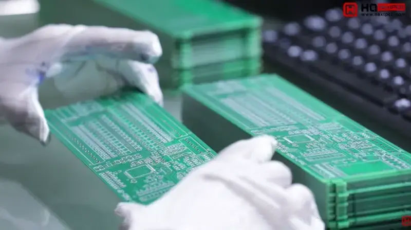
The copper pattern is formed by imaging the panel with a resist and then etching away the unwanted copper in a chemical bath. The etchant attacks sideways as well as downwards, so the width of the trace at the top of the foil is narrower than at the base; this undercut is the reason minimum line width and minimum spacing have to be quoted together with the copper weight. After etching, the resist is stripped, and the panel receives a solder mask to protect the copper and control where solder can flow, followed by a silkscreen legend and a surface finish that keeps the exposed pads solderable during storage.
Design Rules That Keep the Board Economic
Keep the layout sparse. Minimum trace width and spacing should be quoted at or slightly above the fabricator’s standard capability rather than at the limit, because a board that pushes the process adds cost and reduces yield for no functional gain. Allow generous clearance between the copper pattern and the board edge so the profile router or the punch die does not expose or lift a trace.
Route with the crossing problem in mind. Because the copper is on one face, a wire link or a zero-ohm resistor is the standard way to let two nets cross, and a design that needs only a handful of these is still far cheaper than moving to two layers. Where a link would be unacceptable, the usual alternatives are to reorder the components to remove the crossing or to accept a longer return path, which is often the better answer in low-speed circuits. Our design release checklist covers the items that should be reviewed before the file is released.
Assembly on a Single-Sided Board
Through-hole assembly is the natural fit, since the leads pass through the board and are soldered on the copper side, and wave soldering can handle a whole panel at once. Selective soldering is used where a small number of connectors share the board with surface mount parts on the same face, and hand soldering remains perfectly acceptable for prototypes and small batches.
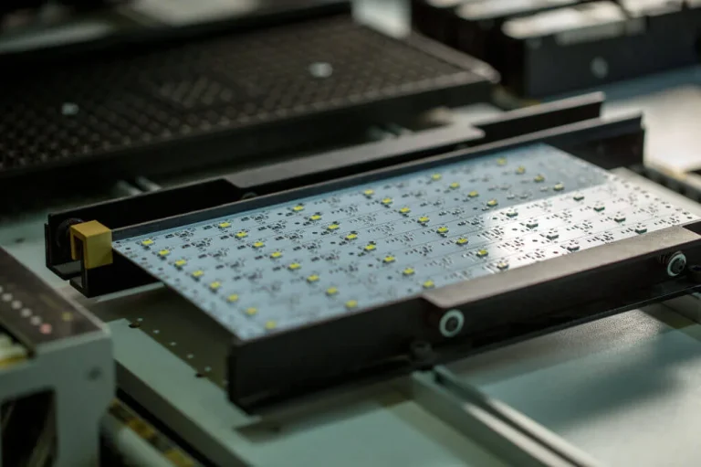
Surface mount parts can also be used, provided the designer accepts that the solder joints, the traces and the components are all on the same side. That is common in LED lighting, where the thermal path from the package into the copper is more important than the density of the routing, and where the single metal face can be turned into a large heat spreading area. Thermal performance in those products is worth checking before the layout is frozen, and our thermal management notes describe how the copper area is estimated.
Testing and Quality Control
Visual inspection under magnification catches most defects in a single-sided product because the entire pattern is visible from one side. Continuity testing verifies that no net is broken and no two nets are shorted, and on a low-density board this can be done with a simple fixture or even by hand on a prototype.
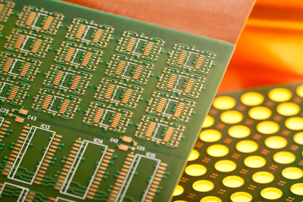
Solderability of the finished surface is checked on samples from each lot, particularly where the boards will be stored for some time before assembly. Where the product carries mains voltage, an isolation and dielectric withstand test is performed on the finished assembly rather than on the bare board, since the creepage distances that matter are the ones created by the assembly as a whole. Our component tolerance and reliability material explains how the mechanical stress on the joints is assessed.
When to Move to Two Layers
The decision is driven by crossings and by current, not by fashion. If the number of wire links grows beyond a handful, or if a single ground net has to snake through the whole board to reach every component, a two-layer board with a ground plane on the back will usually be cheaper once assembly labour is counted.
High-speed signals and controlled impedance settle the question immediately, because both require a continuous reference plane that a single-sided board cannot provide. Below that threshold, and where the circuit is simple enough that the routing can be checked by eye, the single-sided board remains the rational choice. Assuming it is only a stopgap for student projects underestimates how much of the world still runs on one copper layer.
FAQ
Can a single-sided PCB have plated through holes? Not in the usual sense, because plating requires a connection between both faces. Holes are mechanical clearances and the joint is formed by solder on the copper side, unless an eyelet is deliberately crimped and soldered.
How much cheaper is a single-sided board than a two-layer board? The gap is largest at small volumes, where the plating and lamination steps dominate the price. At high volume the difference narrows because panel handling and testing become the main cost, but the single-sided board still leads on lead time.
What is the most common mistake in single-sided layouts? Assuming a trace is a zero-ohm connection. On a single copper layer the return current shares the same limited path as everything else, so the resistance and the loop area grow quickly and cause problems that a two-layer board would hide.