Smart Sensor Circuit Board: Structure and Key Technology
A smart sensor is a device that measures something, processes the measurement and reports a result that has already been interpreted. It differs from an ordinary sensor in that the conversion, the compensation and often the decision logic all sit inside the same housing, which means the circuit board inside it is a complete mixed-signal system rather than a simple transducer interface. A smart sensor circuit board has to deliver a thermally stable environment for the sensing element, a quiet reference for the conversion and a communication interface, all within a package that is often smaller than a coin.
What Makes a Sensor Smart
The distinguishing feature is that the signal is conditioned where it is generated. A conventional sensor returns a raw voltage or current, and the receiver has to compensate for its offset, its temperature coefficient and its non-linearity. A smart sensor performs those corrections locally, using a calibration that was stored in the device at manufacture, and reports a value in engineering units over a digital interface.
That architecture moves the analogue design problem into a much smaller space, which is what makes the layout difficult. The sensing element, the amplifier, the analogue to digital converter and the microcontroller now share a few square centimetres, and the microcontroller’s clock is only millimetres from a node that may be resolving microvolts. The physical separation that a larger instrument would provide is simply not available here, so the isolation has to come from layout, from guard structures and from making a deliberate decision about which circuit owns the reference.
Sensing Elements and the Analogue Front End
The sensing element determines everything downstream. A resistive bridge produces a differential output of a few millivolts and needs a stable excitation; a capacitive element needs an AC excitation and a charge amplifier; a piezoelectric element produces a charge rather than a voltage and needs an amplifier with an extremely high input impedance. Each of those has a different requirement for guarding, for shielding and for the reference that the measurement is made against.
The front end should be treated as its own board within the board. A guard ring around the high impedance node, a separate analogue reference that the digital return does not share, and a conversion reference that is decoupled right at its pin are the measures that preserve accuracy. Where the element and the electronics are on the same laminate, the thermal gradient across the board becomes part of the measurement error, and the layout should place the element so that it sees the same temperature as the compensation circuit. Our component tolerance and reliability notes describe how that error is assessed.
Mixed-Signal Layout Discipline
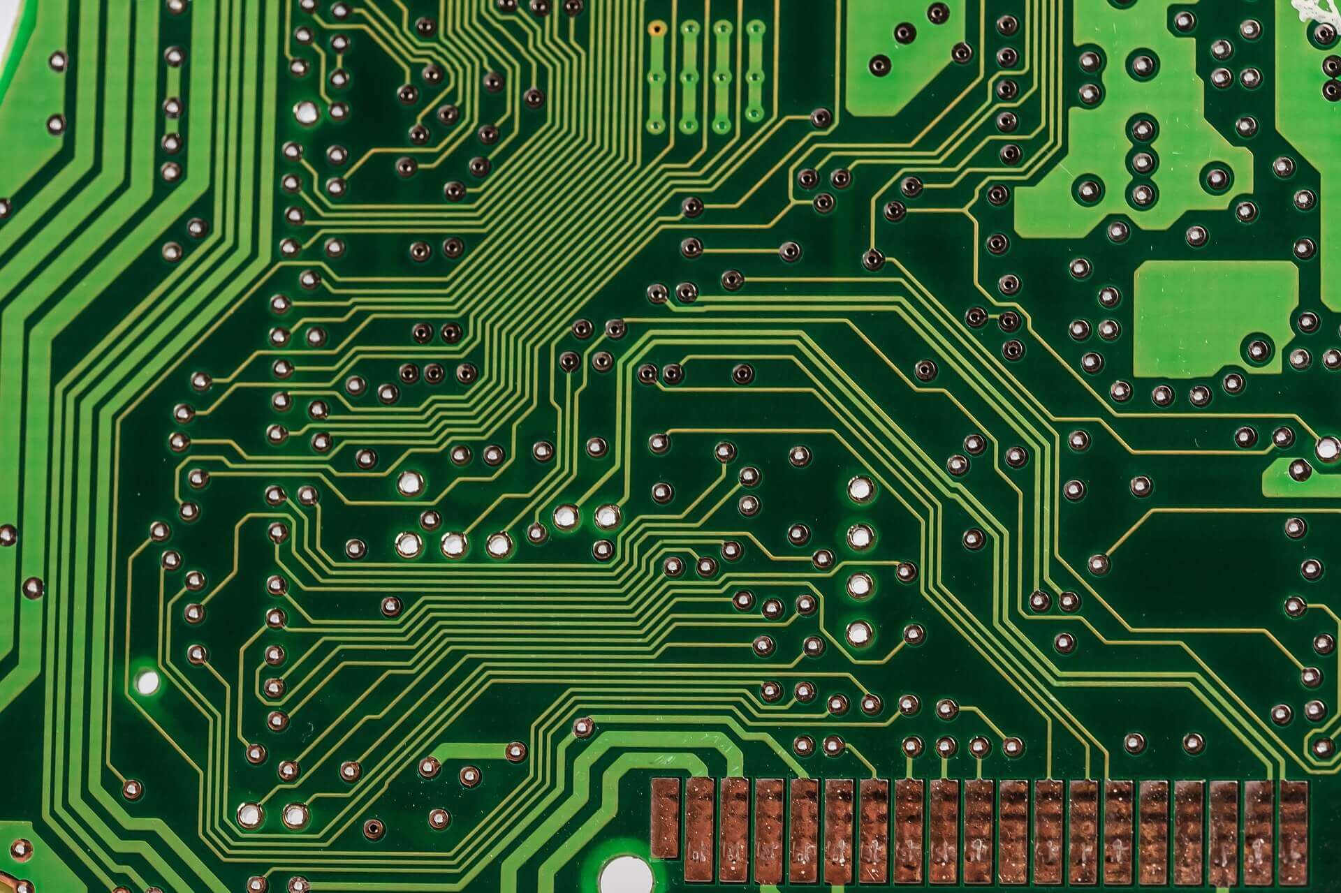
The board carries an analogue section resolving microvolts and a digital section switching at megahertz, and the two must be arranged so that the digital return current does not flow through the analogue reference. The standard approach is a continuous ground plane with the analogue section placed over one area of it and the digital section over another, so that the return currents stay in their own regions because they naturally follow the path of least impedance beneath their traces.
Cutting the plane in two and joining it at a single point is the alternative that is often recommended, and it is correct only when the join is placed so that no signal return has to cross the boundary. When it is placed badly, every digital signal that crosses the gap has to detour around it, and the resulting loop radiates into the very circuit the split was meant to protect. Our layer assignment notes describe how the stack is arranged to make that choice straightforward.

Communication, Power and Enclosure
The communication interface is chosen to suit the installation. A two wire industrial bus is common where the sensor is one of many on a long cable, a differential pair is used where the data rate is higher, and a wireless link is used where cabling is impractical. Each has its own layout requirement, and the interface protection belongs at the connector rather than further into the board.
Power is usually supplied over the same cable as the data, which means the sensor must tolerate a wide input voltage and survive a reverse connection. A switching regulator is more efficient where the drop across a linear regulator would dissipate too much heat in a sealed housing, and its switching noise has to be kept away from the analogue front end by placement and by filtering rather than by hoping that the frequency is out of band.
Calibration, Compensation and Drift
The value of a smart sensor is that it stays accurate. Offset drift, gain drift and the temperature coefficient of the sensing element are corrected using a calibration stored in non-volatile memory, and the accuracy of that correction depends on the stability of the reference against which the measurement is made. A reference with a low initial tolerance but a poor temperature coefficient will produce a sensor that is accurate in the calibration laboratory and wrong in a cold warehouse.
Where the correction requires a temperature measurement, the temperature sensor should be placed so that it sees the same thermal environment as the element rather than the heat of the processor. In a small housing the processor is often the dominant heat source, and placing the temperature sensor next to it produces a correction that compensates for the wrong thing. Our thermal management article describes how that gradient is estimated before the layout is fixed.
Testing and Validation
Functional test covers the measurement chain, the interface and the calibration, and it is usually performed with the sensor exposed to a known stimulus. What matters more is validation across temperature: the same stimulus applied at the extremes of the operating range, with the error recorded, because the compensation that was calculated on the bench is only as good as the data it was derived from.
A long term drift test is also worthwhile where the product must remain accurate for years. It is slow and therefore expensive, which is why it is often replaced by an accelerated test at elevated temperature, but the underlying question is the same: does the sensor still read correctly after the reference has aged and the board has been through a few thousand thermal cycles. Our design release checklist places those checks in the review sequence.
FAQ
Why is a separate analogue reference needed on a smart sensor board? Because the measurement is a comparison against that reference. If the reference is taken from a supply that also feeds the processor, every current step in the processor appears as a measurement error.
Can the sensing element share a board with the processor? Yes, and it usually does, but the element needs its own quiet area of copper and its own thermal environment. The layout has to keep the processor’s heat and its return currents away from it.
What limits accuracy more, the electronics or the element? In a well designed product the element and its temperature behaviour dominate. The board’s job is to avoid adding error on top of that, which is mostly a matter of reference stability and thermal gradient.