Smart Sensor PCB Guide: Structure, Working Principles and Manufacturing
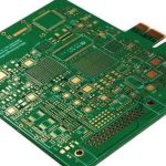
Smart devices, wearable monitors, industrial sensors, and connected cars all share a common foundation: the smart sensor PCB. As electronic systems move toward real-time data collection, efficient processing, and autonomous decision-making, these circuit boards integrate sensing elements, signal processing, wireless communication, power management, and control algorithms on a single platform. This smart sensor PCB guide explains what these boards are, how they are structured, how they work, what they cost, and what to consider when manufacturing them for IoT, medical, industrial, and automotive applications.
What Is a Smart Sensor PCB?
A smart sensor PCB is a circuit board that goes beyond carrying raw sensor signals. Unlike a traditional sensor board, which simply routes analog measurements to another processor, a smart sensor board performs local computing, data filtering, self-calibration, and even edge reasoning on board. That local intelligence improves system response speed, lowers power consumption, and increases data reliability, because the device can decide which data is worth sending to the cloud.
With global demand for smart devices rising quickly, the value of intelligent sensor boards is growing just as fast. Products that once needed a separate gateway or hub can now process information locally, which matters for battery-powered sensors that must run for months or years without maintenance.
Core Components of a Smart Sensor PCB
A typical smart sensor PCB brings several building blocks together. MEMS sensors measure physical quantities such as pressure, temperature, acceleration, or humidity. A microcontroller or DSP handles local processing and decision logic. Analog front-end circuits amplify and filter weak sensor signals before conversion. Wireless modules provide BLE, Wi-Fi, or LoRa connectivity, and voltage regulators and power switching devices manage the energy budget.
Working together, these modules capture environmental data, convert it into usable information, and deliver intelligent output to a gateway, cloud service, or local actuator. The balance between sensing performance, processing power, and energy use is what separates a good smart sensor design from one that drains its battery or misses important events.
Structure and Stack-Up Design
Smart sensor boards commonly use 4 to 10 layer constructions to satisfy signal isolation and routing requirements. Common materials include FR-4 epoxy laminate for general use, polyimide flexible material for bendable sections, and high-Tg laminates for high-temperature environments. For wearables, rigid-flex construction is increasingly preferred because it removes connectors, saves space, and improves reliability under repeated motion.
The stack-up must protect sensitive analog signals from digital noise. Sensor traces are routed on quiet layers, power planes are split carefully, and ground references stay continuous under every analog component. When the physical structure is planned well, a flex PCB assembly partner can build the design without compromising the delicate sensor area.
How a Smart Sensor PCB Works
The operating flow of a smart sensor board is straightforward in concept. First, the sensor detects a physical quantity and converts it into an electrical signal. The analog front end amplifies the signal and filters out noise. An ADC converts the analog value into digital form, and the microcontroller processes and analyzes the data. Finally, the wireless module uploads results to a cloud service or local gateway.
This architecture keeps data fresh and accurate while limiting communication to meaningful events. In a predictive maintenance system, for example, the board monitors vibration continuously but only reports when patterns change. That approach cuts bandwidth costs dramatically and keeps the system responsive.
Data Acquisition and Signal Conditioning
High-accuracy measurement starts with clean signals. Designers commonly use low-pass filters to remove high-frequency interference, notch filters to suppress power-line noise, and programmable gain amplifiers to match the sensor output range to the ADC input. The quality of this analog chain directly determines how stable and repeatable the sensor readings are.
Careful layout is just as important as the filter design. Analog traces must be short and shielded from clock lines, and the ground return paths must not be shared with switching power circuits. Small improvements in the analog front end often produce larger gains in accuracy than upgrading the sensor itself.
Communication and Connectivity Technologies
Smart sensor PCBs support a wide range of wireless protocols. BLE 5.0 offers low-power communication for battery devices such as tags and wearable sensors. Wi-Fi 6 handles larger data volumes for cameras and gateways. LoRa provides extremely long-range links for agricultural and industrial monitoring, while UWB and NFC cover short-range precise positioning and pairing. Many boards include two radios so they can act as both sensor node and gateway.
Wireless integration adds complexity to the board design. Antenna clearance, RF shielding, and impedance matching must be handled correctly or the radio range drops noticeably. Choosing the right module and antenna strategy early in the design avoids the most common connectivity failures in field deployments.
Power Management Strategies
Low power consumption is one of the most important design goals for smart sensor boards. Engineers use MCU deep sleep with low-frequency wake-up timers, combine LDO and buck converters to match each voltage rail to its load, harvest energy from light, heat, or vibration where possible, and apply dynamic voltage scaling to reduce consumption during light workloads.
These techniques can extend battery life from weeks to years for the same sensor function. Power management is designed together with the radio schedule: the board sleeps most of the time, wakes briefly to take a measurement, transmits a short packet, and returns to sleep. Every microamp saved in sleep mode multiplies into months of additional field life.

Miniaturization and Integration Challenges
As product size shrinks, smart sensor boards face harder constraints. Routing space becomes scarce, electromagnetic interference increases as traces crowd together, heat accumulates in smaller areas, and components experience greater mechanical stress. Meeting these challenges demands strong layout skill, careful via planning, and disciplined component placement.
High-density designs also require capable manufacturing. Fine-pitch soldering, small via structures, and precise assembly are needed to build compact sensor modules reliably. Factories experienced in SMT PCB assembly of miniature IoT hardware understand how to manage the yield risks of dense sensor boards.
Key Technologies Driving Smart Sensor PCBs
Several technology trends are pushing smart sensor boards forward. Highly integrated MEMS devices now combine multiple sensing axes in tiny packages. Microcontrollers with built-in AI inference run pattern recognition without a cloud connection. Ultra-low-power RF transceivers shrink the energy cost of connectivity, and edge computing firmware keeps improving in capability. Future systems will gain stronger self-learning behavior, adapting their thresholds and reporting patterns to the environment automatically.
Typical Application Areas
Smart sensor PCBs serve markets that keep expanding. In smart homes they handle temperature, humidity, presence, and air-quality sensing. In industry they monitor machine vibration and gas levels for predictive maintenance. In medical wearables they support blood oxygen, ECG, and posture analysis. In automotive electronics they enable ADAS features such as blind-spot detection and thermal imaging. For industrial deployments, boards can be paired with robust enclosure and protection options through industrial PCBA services that account for harsh operating conditions.
Reliability and Environmental Protection
Smart sensors often live in demanding environments, so protection is part of the board design. Conformal coating shields circuitry from moisture and contamination, IP67 and IP68 enclosures keep out dust and water, corrosion-resistant finishes protect contact surfaces, and UV-resistant solder mask extends outdoor life. Together these measures let a board serve reliably for years in locations that would destroy unprotected electronics in weeks.
Common Faults and Troubleshooting
Even well-designed sensor boards can develop problems. Thermal drift reduces measurement accuracy as temperature changes, vibration causes solder joint fatigue in moving equipment, EMI introduces noise into readings, and aging capacitors degrade filter performance. During development, AOI and X-ray inspection help engineers find assembly defects, while long-duration testing reveals drift and intermittent issues before mass production.
Manufacturing Considerations
Producing smart sensor boards requires attention beyond standard PCB fabrication. Fine-pitch soldering must be controlled precisely for small sensor packages. Sensor calibration procedures ensure each board reports consistent values. Small-batch, multi-variant production capability matters because sensor products often ship in many configurations. Automated test equipment verifies each unit quickly and repeatably, and medical-grade products demand especially careful accuracy calibration. A complete PCBA testing program that includes ICT, functional checks, and calibration records protects both yield and field reliability.

Smart Sensor PCB Cost Factors
Cost depends on layer count and material grade, component density and package style, wireless module selection, and protection requirements such as waterproofing. As a reference, a basic single-sensor board typically costs USD 12 to USD 25, a multi-sensor IoT module runs from USD 28 to USD 65, and a miniature medical wearable board ranges from USD 70 to USD 120. Certification costs for CE, FCC, or UL add to the project budget but are unavoidable for commercial products.
For volume production, gopcb manufactures rigid, flexible, and rigid-flex smart sensor boards with standard pricing around USD 0.12 to USD 0.25 per square centimeter depending on process difficulty and batch size. Component sourcing can be bundled through components procurement services so the BOM arrives coordinated with board production, which simplifies logistics and protects the schedule.
Future Trends in Smart Sensor PCB Technology
The next generation of smart sensor boards will continue to evolve. On-board neural network processing will bring real-time recognition to battery devices, multimodal sensing will combine sound, motion, and environmental data in one system, fully flexible 3D packaging will fit sensors into new form factors, and adaptive calibration algorithms will keep accuracy stable over time. Edge AI is moving these boards from simple data reporters to autonomous decision makers.
Prototype runs also play a critical role in sensor board programs. A short first batch lets engineers verify calibration, radio performance, and power consumption with real hardware before committing to mass production. Quick-turn prototyping is especially valuable for medical and automotive projects where the qualification cycle is long and design changes late in the program are expensive. Planning two validation rounds in the schedule, one for electrical performance and one for environmental reliability, is a proven pattern for sensor products that must work correctly on the first field deployment.
Smart Sensor PCB FAQ
Q1: What is the difference between a smart sensor PCB and a traditional sensor board? A smart sensor board has local processing and decision-making ability, while a traditional board only delivers raw signals to another processor.
Q2: How long does a smart sensor PCB last? Typical service life is 5 to 12 years depending on the operating environment and protection measures.
Q3: Can smart sensor boards be made waterproof? Yes, potting, conformal coating, and sealed encapsulation can achieve IP67 and above.
Q4: How can EMI noise be reduced? Adding ground planes, stitching vias, and using differential routing all effectively suppress interference.
Q5: What does a smart sensor PCB cost? Basic boards start around USD 12, and medical wearable designs can reach USD 120 depending on complexity.
Conclusion
The smart sensor PCB is a core foundation of modern intelligent systems. Its modular, highly integrated, low-power, and precise nature makes it suitable for automation, healthcare, IoT, and automotive safety applications. As technology advances, these boards will become more capable, smaller, and more reliable, and teams that understand their structure, cost drivers, and manufacturing requirements will be best positioned to build the next generation of connected products.