USB-C Hub Design: PD Negotiation, Alt Mode and Routing
A USB-C hub or dock looks like a small accessory and contains problems from several disciplines at once. It negotiates power with the host, it switches video lanes between two protocols, it carries multi-gigabit differential pairs through connectors and PCB traces, and it does all of it inside a metal enclosure with no fan. Each of those is a separate design exercise, and they share the same few square centimetres of board.
The product specification usually arrives as a list of ports and a maximum resolution. Turning that into a board means deciding what the controller can do, what the connector must support, and how the power and the heat will be handled before the layout begins.
Start With the Power Contract
The first question is how much power the hub passes through and how much it consumes. A dock that charges the host while running a display, a network interface and two storage devices has to negotiate a contract with the host, allocate what the internal functions need, and pass the remainder to the charging port. Power delivery negotiation is therefore part of the architecture, not a firmware detail.
Practically, that means the input path has to carry the negotiated voltage and current without an excessive drop, the internal rails have to be generated from that input efficiently, and every port has to be protected against the case where a user connects something that draws more than the budget allows. A port that can supply a defined current needs its own current limiting, because the host cannot be relied on to protect a device that the hub itself is powering.

Alternate Mode and Video Output
Video over USB-C uses the connector Alt Mode, in which the high speed lanes are re-purposed for a display protocol. The controller has to detect what has been connected, negotiate the mode, and configure the switch that routes the lanes to the appropriate output. Whether the hub supports a single output, two outputs at reduced resolution, or a display port converted internally to HDMI, follows from the capabilities of that controller and must be settled before the schematic is drawn.
The switching network is where signal integrity is won or lost. Every switch adds capacitance and a small discontinuity, and a path that passes through a connector, a switch, a level of vias and another connector accumulates loss and reflections. The controller datasheet usually provides the required routing rules, including the maximum trace length for each interface, the permitted loss and the reference plane requirements, and those rules should be treated as limits rather than suggestions. The stack-up that provides the controlled impedance is a question for the board supplier and has to be agreed before the layout is finished.
Routing the High Speed Pairs
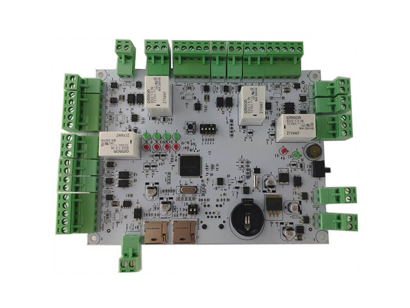
Differential pair routing on a board of this kind means a consistent width and gap, kept on a single layer for as much of their length as possible, and referred to a continuous ground plane. A pair that changes layer twice needs two via structures, and both of them have to be treated as impedance discontinuities with the correct antipad geometry and, where the stub would be significant, with a back drill or a blind via to remove it.
Length matching matters within each pair, and skew between the two halves of the pair turns part of the differential signal into an unwanted common mode component. Between pairs of the same interface, the intra pair skew rules from the controller govern. Also worth remembering is that the connector itself contributes loss, and a cheap connector can consume a large fraction of the total budget before the trace has been considered, so the connector selection is part of the channel design.
The layout should also keep the switching converter away from the high speed channels. A converter’s switching node is a source of both electric and magnetic fields, and on a board this small the distance between the converter and a pair is measured in millimetres. Placing the power section at the opposite end of the board and orienting its loop away from the signal path is the cheapest improvement available.
Thermal Design in a Sealed Enclosure
A metal enclosure with no airflow leaves the board as the only heat spreader, and the dominant heat sources are the controller, the power switches and any linear regulator. The board should be designed so that those devices sit near the enclosure wall or near a thermal pad that couples to it, and the copper beneath them should be extensive, connected through thermal vias to the inner layers and the opposite side.
An aluminium body can also be used as a heat sink deliberately, with a thermal interface material between the device and the case. That decision affects the mechanical design, the assembly sequence and the choice of components, so it belongs with the electrical design rather than after it. A hub that works on a bench and throttles inside its case has been designed without a thermal model.
Protection, EMI and the Things the User Will Do
Users connect whatever is available, hot plug devices repeatedly, and use cables of unknown quality. Input protection should therefore include electrostatic discharge devices at every exposed connector, positioned so that the transient reaches them before the controller, with a short return path. Overcurrent protection belongs on every port that can source power, and the circuitry should recover from a fault without requiring the user to disconnect the host. The connectors themselves are a purchased component whose loss and mechanical life vary by supplier, so their specification belongs in the channel budget.
Emissions are influenced by the same geometry. The high speed pairs and the switching regulators should be kept apart, the return paths should be continuous, and any filtering should be defined by measurement rather than copied. A dock has to pass the emissions and immunity requirements that apply to its market, and those tests are usually performed on the finished product in its enclosure, which means the layout and the mechanical design interact with the compliance result.
Finally, the testing of the assembled product should cover the behaviours that the specification implies: every combination of ports in use, the highest resolution the display supports, charging while the ports are loaded, and disconnection of each device while the rest continue to work. On a device with this many interfaces the failures appear in combination rather than individually, and only a test plan that exercises combinations will find them.
FAQ
Why does the hub support only 4K at 30 Hz? Because the display lanes available through alternate mode and the capabilities of the controller set a bandwidth ceiling, and the highest resolution depends on how many other functions share the link.
Does the power the hub consumes come from the host? It is negotiated. When a charger is connected, the hub can allocate part of the incoming power to itself and pass the remainder to the host.
Do high speed pairs need a different stack-up? They need a controlled impedance stack-up with a defined reference plane, which usually means a multilayer board even for a small product.
Can the aluminium case be used as the heat sink? Yes, and doing so deliberately is better than discovering that the case is the only thermal path after the product has been assembled.
Summary
USB-C hub design starts with the power contract and the video mode, because those decide the controller and the switching network. The high speed pairs then have to be routed within the loss and skew budget the controller specifies, the power section has to be kept away from the signal path, and the thermal design has to assume the enclosure the product will actually be built in. Settle those four, and the list of ports becomes a product rather than a promise.